NCP110
NCP110 is Low Noise and High PSRR Linear Regulator manufactured by onsemi.
DATA SHEET .onsemi.
Linear Regulator
- Low VIN, Low Noise, High PSRR
200 mA
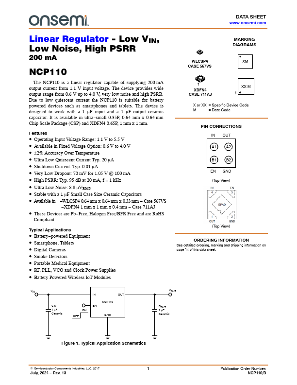
The NCP110 is a linear regulator capable of supplying 200 mA output current from 1.1 V input voltage. The device provides wide output range from 0.6 V up to 4.0 V, very low noise and high PSRR. Due to low quiescent current the NCP110 is suitable for battery powered devices such as smartphones and tablets. The device is designed to work with a 1 mF input and a 1 mF output ceramic capacitor. It is available in ultra- small 0.35P, 0.64 mm x 0.64 mm Chip Scale Package (CSP) and XDFN4 0.65P, 1 mm x 1 mm.
Features
- Operating Input Voltage Range: 1.1 V to 5.5 V
- Available in Fixed Voltage Option: 0.6 V to...