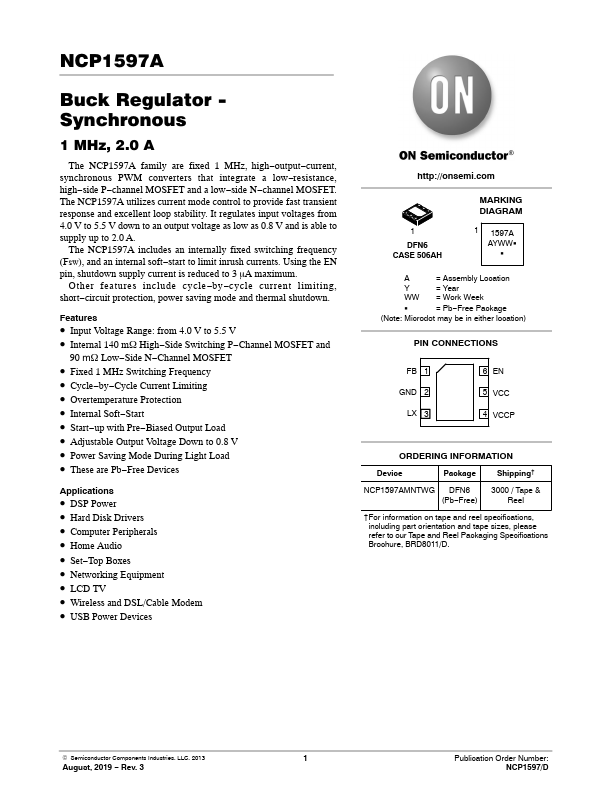
Datasheet4U Logo Datasheet4U.com

NCP1597A - 2.0A Synchronous Buck Regulator

Datasheet Summary

Description

Figure 1.

Description Feedback input pin of the Error Amplifier.

Connect a resistor divider from the converter’s output voltage to this pin to set the converter’s output voltage.

Features

  • include cycle.
  • by.
  • cycle current limiting, short.
  • circuit protection, power saving mode and thermal shutdown. Features.
  • Input Voltage Range: from 4.0 V to 5.5 V.
  • Internal 140 mW High.
  • Side Switching P.
  • Channel MOSFET and 90 mW Low.
  • Side N.
  • Channel MOSFET.
  • Fixed 1 MHz Switching Frequency.
  • Cycle.
  • by.
  • Cycle Current Limiting.
  • Overtemperature Protection.
  • Internal Soft.
  • Start.

📥 Download Datasheet

Datasheet preview – NCP1597A

Datasheet Details

Part number NCP1597A
Manufacturer ON Semiconductor
File Size 556.72 KB
Description 2.0A Synchronous Buck Regulator
Datasheet download datasheet NCP1597A Datasheet
Additional preview pages of the NCP1597A datasheet.
Other Datasheets by ON Semiconductor

Full PDF Text Transcription

Click to expand full text
NCP1597A Buck Regulator - Synchronous 1 MHz, 2.0 A The NCP1597A family are fixed 1 MHz, high−output−current, synchronous PWM converters that integrate a low−resistance, high−side P−channel MOSFET and a low−side N−channel MOSFET. The NCP1597A utilizes current mode control to provide fast transient response and excellent loop stability. It regulates input voltages from 4.0 V to 5.5 V down to an output voltage as low as 0.8 V and is able to supply up to 2.0 A. The NCP1597A includes an internally fixed switching frequency (FSW), and an internal soft−start to limit inrush currents. Using the EN pin, shutdown supply current is reduced to 3 mA maximum. Other features include cycle−by−cycle current limiting, short−circuit protection, power saving mode and thermal shutdown.
Published: |