NCP177
NCP177 is Low Voltage Regulator manufactured by onsemi.
Linear Voltage Regulator Fast Transient Response, Enable
500 m A
The NCP177 is CMOS LDO regulator featuring 500 m A output current. The input voltage is as low as 1.6 V and the output voltage can be set from 0.7 V.
Features
- Operating Input Voltage Range: 1.6 V to 5.5 V
- Output Voltage Range: 0.7 V to 3.6 V
- Quiescent Current typ. 60 m A
- Low Dropout: 200 m V Typ. at 500 m A, VOUT- NOM = 1.8 V
- High Output Voltage Accuracy ±0.8%
- Stable with Small 1 m F Ceramic Capacitors
- Over- current Protection
- Thermal Shutdown Protection: 175°C
- With (NCP177A) and Without (NCP177B) Output Discharge
Function
- Available in XDFN4 1 mm x 1 mm x 0.4 mm Package
- This is a Pb- Free Device
Typical Applications
- Battery Powered Equipment
- Portable munication Equipment
- Cameras, Image Sensors and Camcorders
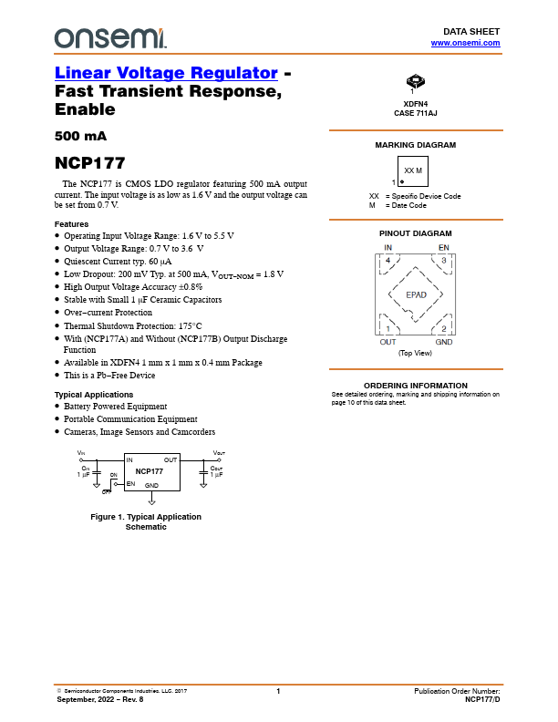
VIN CIN
1 μF
ON OFF
EN GND
VOUT COUT 1 μF
Figure 1. Typical Application Schematic
DATA SHEET .onsemi.
1 XDFN4 CASE 711AJ MARKING DIAGRAM XX M 1 XX = Specific Device Code M = Date Code PINOUT DIAGRAM
(Top View)
ORDERING...