NCP3418B
NCP3418B is MOSFET Driver manufactured by onsemi.
..
NCP3418B MOSFET Driver with Dual Outputs for Synchronous Buck Converters
The NCP3418B is a single Phase 12 V MOSFET gate driver optimized to drive the gates of both high- side and low- side power MOSFETs in a synchronous buck converter. The high- side and low- side driver is capable of driving a 3000 p F load with a 25 ns propagation delay and a 20 ns transition time. With a wide operating voltage range, high or low side MOSFET gate drive voltage can be optimized for the best efficiency. Internal adaptive nonoverlap circuitry further reduces switching losses by preventing simultaneous conduction of both MOSFETs. The floating top driver design can acmodate VBST voltages as high as 30 V, with transient voltages as high as 35 V. Both gate outputs can be driven low by applying a low logic level to the Output Disable (OD) pin. An Undervoltage Lockout function ensures that both driver outputs are low when the supply voltage is low, and a Thermal Shutdown function provides the IC with overtemperature protection. The NCP3418B is pin- to- pin patible with Analog Devices ADP3418 with the following advantages:
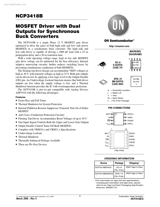
Features http://onsemi. MARKING DIAGRAMS
8 8 1 SO- 8 D SUFFIX CASE 751 1 3418B ALYW G
DFN- 10 MN SUFFIX CASE 485C A L Y W G = Assembly Location = Wafer Lot = Year = Work Week = Pb- Free Package
3418B ALYW G
- Faster Rise and Fall Times
- Thermal Shutdown for System Protection
- Internal Pulldown Resistor Suppresses Transient Turn On of Either
- -
- -
- -
- -
- MOSFET Anti Cross- Conduction Protection Circuitry Floating Top Driver Acmodates Boost Voltages of up to 30 V One Input Signal Controls Both the Upper and Lower Gate Outputs Output Disable Control Turns Off Both MOSFETs plies with VRM10.x and VRM11.x Specifications Undervoltage Lockout Thermal Shutdown Thermally Enhanced Package Available These are Pb- Free Devices
PIN CONNECTIONS
BST IN OD VCC 1 BST IN OD VCC VCC (Top View) 10 DRVH SWN PGND PGND DRVL 1 8 DRVH SWN PGND DRVL
ORDERING...