Datasheet4U Logo Datasheet4U.com

NCP5109B - High and Low Side Driver

Download the NCP5109B datasheet PDF. This datasheet also covers the NCP5109A variant, as both devices belong to the same high and low side driver family and are provided as variant models within a single manufacturer datasheet.

General Description

Pin Name ÁÁÁÁÁÁÁÁÁÁÁÁÁÁÁÁÁÁÁÁÁÁÁÁ IN_HI ÁÁÁÁÁÁÁÁÁÁÁÁÁÁÁÁÁÁÁÁÁÁÁÁ IN_LO ÁÁÁÁÁÁÁÁÁÁÁÁÁÁÁÁÁÁÁÁÁÁÁÁ GND ÁÁÁÁÁÁÁÁÁÁÁÁÁÁÁÁÁÁÁÁÁÁÁÁ DRV_LO ÁÁÁÁÁÁÁÁÁÁÁÁÁÁÁÁÁÁÁÁÁÁÁÁ VCC ÁÁÁÁÁÁÁÁÁÁÁÁÁÁÁÁÁÁÁÁÁÁÁÁ VBOOT ÁÁÁÁÁÁÁÁÁÁÁÁÁÁÁÁÁÁÁÁÁÁÁÁ DRV_HI ÁÁÁÁÁÁÁÁÁÁÁÁÁÁÁÁÁÁÁÁÁÁÁÁ BRIDGE ÁÁÁÁÁÁÁÁÁÁÁÁÁÁÁÁÁÁÁÁÁÁÁÁÁÁÁÁÁÁÁÁÁÁÁÁÁÁÁÁÁÁÁ

Key Features

  • High Voltage Range: Up to 200 V.
  • dV/dt Immunity 50 V/nsec.
  • Negative Current Injection Characterized Over the Temperature Range.
  • Gate Drive Supply Range from 10 V to 20 V.
  • High and Low Drive Outputs.
  • Output Source / Sink Current Capability 250 mA / 500 mA.
  • 3.3 V and 5 V Input Logic Compatible.
  • Up to VCC Swing on Input Pins.
  • Extended Allowable Negative Bridge Pin Voltage Swing to.
  • 10 V for Signal Propagation.
  • Matched Propagation Delays Be.

📥 Download Datasheet

Note: The manufacturer provides a single datasheet file (NCP5109A-ONSemiconductor.pdf) that lists specifications for multiple related part numbers.

Datasheet Details

Part number NCP5109B
Manufacturer onsemi
File Size 280.14 KB
Description High and Low Side Driver
Datasheet download datasheet NCP5109B Datasheet

Full PDF Text Transcription (Reference)

The following content is an automatically extracted verbatim text from the original manufacturer datasheet and is provided for reference purposes only.

View original datasheet text
DATA SHEET www.onsemi.com High Voltage, High and Low Side Driver NCP5109A, NCP5109B 
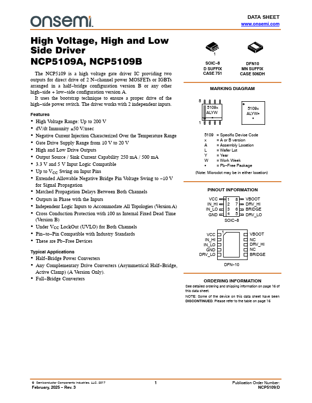
The NCP5109 is a high voltage gate driver IC providing two outputs for direct drive of 2 N−channel power MOSFETs or IGBTs arranged in a half−bridge configuration version B or any other high−side + low−side configuration version A. It uses the bootstrap technique to ensure a proper drive of the high−side power switch. The driver works with 2 independent inputs. Features  High Voltage Range: Up to 200 V  dV/dt Immunity 50 V/nsec  Negative Current Injection Characterized Over the Temperature Range  Gate Drive Supply Range from 10 V to 20 V  High and Low Drive Outputs  Output Source / Sink Current Capability 250 mA / 500 mA  3.