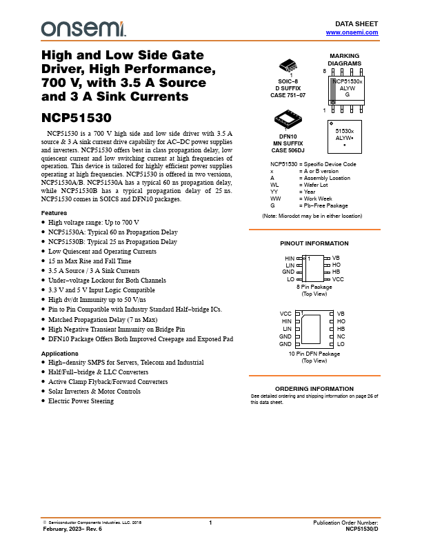
NCP51530
Key Features
- High voltage range: Up to 700 V
- NCP51530A: Typical 60 ns Propagation Delay
- NCP51530B: Typical 25 ns Propagation Delay
- Low Quiescent and Operating Currents
- 15 ns Max Rise and Fall Time
- 3.5 A Source / 3 A Sink Currents
- Under-voltage Lockout for Both Channels
- High dv/dt Immunity up to 50 V/ns
- Matched Propagation Delay (7 ns Max)
- High Negative Transient Immunity on Bridge Pin
Applications
- Half/Full-bridge & LLC Converters