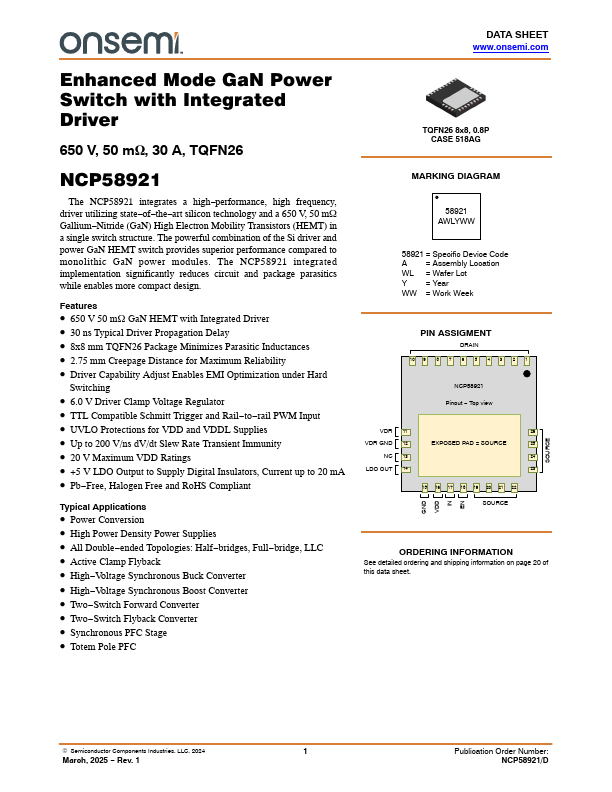
Datasheet4U Logo Datasheet4U.com

NCP58921 - GaN Power Switch

Description

Pin No.

10 DRAIN GaN Power Switch Drain Power path connection for the GaN Switch DRAIN 19 22, SOURCE 23 26 GaN Power Switch Source Power path connection for the GaN Switch SOURCE 11 VDR Driver clamp regulator decoupling Connect

Features

  • 650 V 50 mW GaN HEMT with Integrated Driver.
  • 30 ns Typical Driver Propagation Delay.
  • 8x8 mm TQFN26 Package Minimizes Parasitic Inductances.
  • 2.75 mm Creepage Distance for Maximum Reliability.
  • Driver Capability Adjust Enables EMI Optimization under Hard Switching.
  • 6.0 V Driver Clamp Voltage Regulator.
  • TTL Compatible Schmitt Trigger and Rail.
  • to.
  • rail PWM Input.
  • UVLO Protections for VDD and VDDL Supplies.

📥 Download Datasheet

Datasheet preview – NCP58921

Datasheet Details

Part number NCP58921
Manufacturer ON Semiconductor
File Size 550.44 KB
Description GaN Power Switch
Datasheet download datasheet NCP58921 Datasheet
Additional preview pages of the NCP58921 datasheet.
Other Datasheets by ON Semiconductor

Full PDF Text Transcription

Click to expand full text
DATA SHEET www.onsemi.com Enhanced Mode GaN Power Switch with Integrated Driver 650 V, 50 mW, 30 A, TQFN26 TQFN26 8x8, 0.8P CASE 518AG NCP58921 The NCP58921 integrates a high−performance, high frequency, driver utilizing state−of−the−art silicon technology and a 650 V, 50 mW Gallium−Nitride (GaN) High Electron Mobility Transistors (HEMT) in a single switch structure. The powerful combination of the Si driver and power GaN HEMT switch provides superior performance compared to monolithic GaN power modules. The NCP58921 integrated implementation significantly reduces circuit and package parasitics while enables more compact design. Features • 650 V 50 mW GaN HEMT with Integrated Driver • 30 ns Typical Driver Propagation Delay • 8x8 mm TQFN26 Package Minimizes Parasitic Inductances • 2.
Published: |