NCV8842
NCV8842 is Buck Regulator manufactured by onsemi.
1.5 A, 170 k Hz, Buck Regulator with Synchronization Capability
The NCV8842 is a 1.5 A buck regulator IC operating at a fixed- frequency of 170 k Hz. The device uses the V2t control architecture to provide unmatched transient response, the best overall regulation and the simplest loop pensation for today’s high- speed logic. The NCV8842 acmodates input voltages from 4.0 V to 40 V and contains synchronization circuitry.
The on- chip NPN transistor is capable of providing a minimum of 1.5 A of output current, and is biased by an external “boost” capacitor to ensure saturation, thus minimizing on- chip power dissipation. Protection circuitry includes thermal shutdown, cycle- by- cycle current limiting and frequency foldback.
Features
- V2 Architecture Provides Ultra- Fast Transient Response, Improved
Regulation and Simplified Design
- Wide Operating Range: 4 V to 40 V
- 2.0% Error Amp Reference Voltage Tolerance
- Switch Frequency Decrease of 4:1 in Short Circuit Conditions
Reduces Short Circuit Power Dissipation
- BOOST Lead Allows “Bootstrapped” Operation to Maximize
Efficiency
- Sync Function for Parallel Supply Operation or Noise Minimization
- Shutdown Lead Provides Power- Down Option
- 1.0 m A Quiescent Current During Power- Down
- Thermal Shutdown
- Soft- Start
- Exposed Pad Packages for Enhanced Thermal Characteristics
- NCV Prefix for Automotive and Other Applications Requiring Site and Change Controls
- These are Pb- Free Devices http://onsemi.
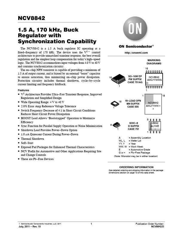
MARKING DIAGRAMS
16 1
SO- 16W EP PW SUFFIX CASE 751AG
NCV8842 AWLYYWWG
18 18- LEAD DFN MN SUFFIX CASE 505
NCV8842 AWLYYWW G
8 1
SOIC- 8 D SUFFIX CASE 751
V8842 ALYWE
G...