NLHVQ011
Features
- Gate Pulse Modulation (GPM)
- AEC- Q100 Grade 1 Qualified
- Adjustable TFT LCD Flicker pensation Circuitry
- Reduction of Coupling Effect Between Gate Line and Pixel
- Provides Power Sequencing Circuit for Gate Driver IC
- Wide Power Supply Operation: 15 V to 38 V
- Output Delay and Fall Time are Independently Adjustable
- These Devices are Pb- Free, Halogen Free/BFR Free and are Ro HS pliant
Typical Applications
- TFT LCDs
Important Information
- ESD Protection for All Pins:
Human Body Model (HBM) > 3000 V
.onsemi.
MARKING DIAGRAM
US8 US SUFFIX CASE 493
A3 MG G
A3
= Device Code
= Date Code-
= Pb- Free Package
(Note: Microdot may be in either location)
- Date Code orientation may vary depending upon manufacturing location.
ORDERING INFORMATION
See detailed ordering and shipping information on page 10 of this data sheet.
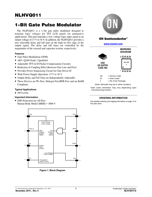
VGH 1
VGH_M 2
High Voltage Power Supply
High Voltage Output Signal
Low Voltage
Input Signal
RE 3
CE 4
Falling Edge Control
Low Voltage...