NTGD1100L Overview
Key Specifications
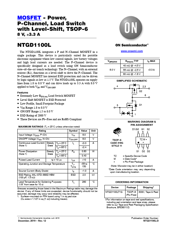
Package: SC
Pins: 6
Height: 1.1 mm
Length: 3.1 mm
Key Features
- Extremely Low RDS(on) Load Switch MOSFET
- Level Shift MOSFET is ESD Protected
- Low Profile, Small Footprint Package
- VIN Range 1.8 to 8.0 V
- ON/OFF Range 1.5 to 8.0 V
- ESD Rating of 2000 V
- These Devices are Pb-Free and are RoHS Compliant