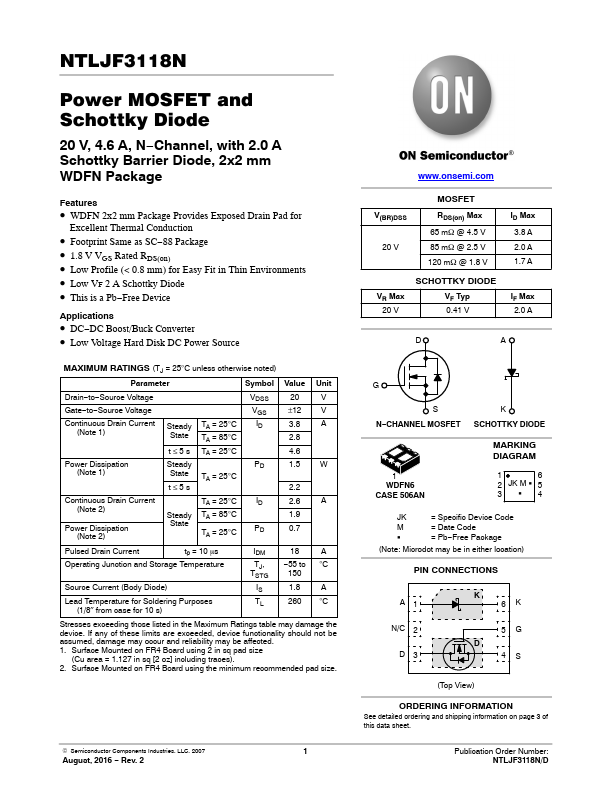
Full PDF Text Transcription for NTLJF3118N (Reference)
Note: Below is a high-fidelity text extraction (approx. 800 characters) for
NTLJF3118N. For precise diagrams, and layout, please refer to the original PDF.
NTLJF3118N Power MOSFET and Schottky Diode 20 V, 4.6 A, N−Channel, with 2.0 A Schottky Barrier Diode, 2x2 mm WDFN Package Features • WDFN 2x2 mm Package Provides Exposed ...
View more extracted text
, 2x2 mm WDFN Package Features • WDFN 2x2 mm Package Provides Exposed Drain Pad for Excellent Thermal Conduction • Footprint Same as SC−88 Package • 1.8 V VGS Rated RDS(on) • Low Profile (< 0.8 mm) for Easy Fit in Thin Environments • Low VF 2 A Schottky Diode • This is a Pb−Free Device Applications • DC−DC Boost/Buck Converter • Low Voltage Hard Disk DC Power Source MAXIMUM RATINGS (TJ = 25°C unless otherwise noted) Parameter Symbol Value Unit Drain−to−Source Voltage VDSS 20 V Gate−to−Source Voltage VGS ±12 V Continuous Drain Current Steady TA = 25°C ID (Note 1) State TA = 85°C 3.8 A 2.8 t ≤ 5 s TA = 25°C 4.