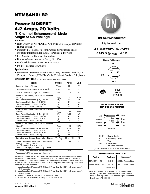
NTMS4N01R2
NTMS4N01R2 is Power MOSFET manufactured by onsemi.
Features
- High Density Power MOSFET with Ultra Low RDS(on) Providing
Higher Efficiency
- Miniature SO- 8 Surface Mount Package Saving Board Space;
Mounting Information for the SO- 8 Package is Provided
- IDSS Specified at Elevated Temperature
- Drain- to- Source Avalanche Energy Specified
- Diode Exhibits High Speed, Soft Recovery
- Pb- Free Package is Available
Applications
- Power Management in Portable and Battery- Powered Products, i.e.: puters, Printers, PCMCIA Cards, Cellular & Cordless Telephones
MAXIMUM RATINGS (TJ = 25°C unless otherwise noted)
Rating
Symbol Value
Unit
Drain- to- Source Voltage
Drain- to- Gate Voltage (RGS = 1.0 m W)
Gate- to- Source Voltage
- Continuous
Thermal Resistance, Junction- to- Ambient (Note 1) Total Power Dissipation @ TA = 25°C Continuous Drain Current @ 25°C Continuous Drain Current @ 70°C Pulsed Drain Current (Note 4)
Thermal Resistance, Junction- to- Ambient (Note 2) Total Power Dissipation @ TA = 25°C Continuous Drain Current @ 25°C Continuous Drain Current @ 70°C Pulsed Drain Current (Note 4)
Thermal Resistance, Junction- to- Ambient (Note 3) Total Power Dissipation @ TA = 25°C Continuous Drain Current @ 25°C Continuous Drain Current @ 70°C Pulsed Drain Current (Note 4)
Operating and Storage Temperature Range
Single Pulse Drain- to- Source Avalanche Energy
- Starting TJ = 25°C (VDD = 20 Vdc, VGS = 5.0 Vdc, Peak IL = 7.5 Apk, L = 6 m H, RG = 25 W)
Maximum Lead Temperature for Soldering Purposes, 1/8″ from case for 10 seconds
VDSS VDGR VGS
Rq JA PD ID ID IDM
Rq JA PD ID ID IDM
Rq JA PD ID ID IDM TJ, Tstg EAS
20 20 ±10
50 2.5 5.9 4.7 25
100 1.25 4.2 3.3 20
162 0.77 3.3 2.6 15
- 55 to +150 169
°C/W W A A A
°C/W W A A A
°C/W W A A A °C m...