NTNS5K0P021Z
NTNS5K0P021Z is P-Channel MOSFET manufactured by onsemi.
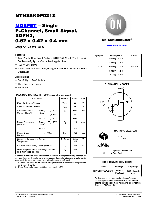
Features
- Low Profile Ultra Small Package, XDFN3 (0.62 x 0.42 x 0.4 mm) for Extremely Space- Constrained Applications
- - 1.5 V Gate Drive
- These Devices are Pb- Free, Halogen Free/BFR Free and are Ro HS pliant
Applications
- Small Signal Load Switch
- High Speed Interfacing
- Level Shift
MAXIMUM RATINGS (TJ = 25°C unless otherwise stated)
Parameter
Symbol Value Unit
Drain- to- Source Voltage
Gate- to- Source Voltage
Continuous Drain Current (Note 1)
Steady State
Power Dissipation (Note 1) t≤5s
Steady State
TA = 25°C TA = 85°C TA = 25°C TA = 25°C
VDSS VGS ID
±8
- 127 m A
- 91
- 146
125 m W t≤5s
Pulsed Drain Current tp = 10 ms
- 488 m A
Operating Junction and Storage Temperature
TJ, TSTG
- 55 to °C 150
Source Current (Body Diode) (Note 2)
Lead Temperature for Soldering Purposes (1/8” from case for 10 s)
200 m A
260 °C
Stresses exceeding those listed in the Maximum Ratings table may damage the device. If any of these limits are exceeded, device functionality should not be assumed, damage may occur and reliability may be affected. 1. Surface- mounted on FR4 board using the minimum remended pad size, or 2 mm2, 1 oz Cu. 2. Pulse Test: pulse width ≤ 300 ms, duty cycle ≤...