NUP4012PXV6 Overview
Key Specifications
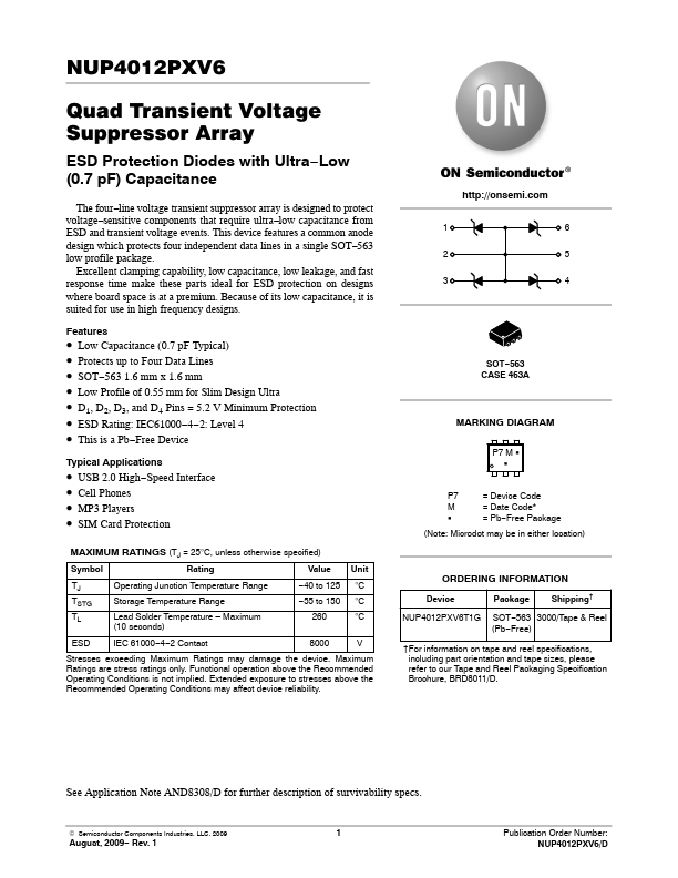
Package: SOT-563
Mount Type: Surface Mount
Pins: 6
Operating Voltage: 4 V
Key Features
- Low Capacitance (0.7 pF Typical)
- Protects up to Four Data Lines
- SOT-563 1.6 mm x 1.6 mm
- Low Profile of 0.55 mm for Slim Design Ultra
- D1, D2, D3, and D4 Pins = 5.2 V Minimum Protection
- ESD Rating: IEC61000-4-2: Level 4
- This is a Pb-Free Device