NUP4060AXV6
NUP4060AXV6 is 4 Line Transient Voltage Suppressor Array manufactured by onsemi.
features a mon cathode design which protects four independent lines in a single SOT- 563 package.
Features http://onsemi.
SOT- 563 4- LINE TRANSIENT VOLTAGE SUPPRESSOR
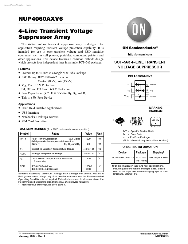
PIN ASSIGNMENT
D1 D2 VCC 1 2 3 6 5 4 GND D3 GND
- Protects up to 4 Lines in a Single SOT- 563 Package
- ESD Rating: IEC61000- 4- 2: Level 4
- -
- -
- -
- Contact (8 k V), Air (15 k V) VCC Pin = 16 V Protection D1, D2, and D3 Pins = 6.8 V Protection Low Capacitance (< 7 p F @ 3 V) for D1, D2, and D3 This is a Pb- Free Device
Applications
Hand Held Portable Applications USB Interface Notebooks, Desktops, Servers SIM Card Protection
MARKING DIAGRAM
6 1 SOT- 563 CASE 463A STYLE 6 MT MG G
MAXIMUM RATINGS (TJ = 25°C, unless otherwise specified)
Symbol PPK 1 Rating Peak Power Dissipation VCC Diode 8x20 msec double exponential waveform, (Note 1) D1, D2, and D3 Operating Junction Temperature Range Storage Temperature Range Lead Solder Temperature
- Maximum (10 seconds) IEC 61000- 4- 2 Air IEC 61000- 4- 2 Contact Value 200 20
- 40 to 125
- 55 to 150 260 15000 8000 Unit W W °C °C °C V
MT = Specific Device Code M = Date Code G = Pb- Free Package (Note: Microdot may be in either location)
TJ TSTG TL ESD
ORDERING INFORMATION
Device Package Shipping†
NUP4060AXV6T1G SOT- 563 4000/Tape & Reel (Pb- Free) †For information on tape and reel specifications, including part orientation and tape sizes, please refer to our Tape and Reel Packaging Specification Brochure, BRD8011/D.
Stresses exceeding Maximum Ratings may damage the device. Maximum Ratings are stress ratings only. Functional operation above the Remended Operating Conditions is not implied. Extended exposure to stresses above the Remended Operating Conditions may affect device reliability. 1. Nonrepetitive current pulse per Figure 1.
© Semiconductor ponents Industries, LLC, 2007
January, 2007
- Rev. 1
Publication Order Number: NUP4060/D
ELECTRICAL CHARACTERISTICS (TJ = 25°C, unless otherwise specified)
Parameter Reverse Working Voltage (D1, D2, and...