Datasheet4U Logo Datasheet4U.com

NVMFD5853NLWF - Power MOSFET

Download the NVMFD5853NLWF datasheet PDF. This datasheet also covers the NVMFD5853NL variant, as both devices belong to the same power mosfet family and are provided as variant models within a single manufacturer datasheet.

Key Features

  • 40 V, 10 mW, 34 A, Dual N.
  • Channel Logic Level, Dual SO.
  • 8FL.
  • Small Footprint (5x6 mm) for Compact Designs Low RDS(on) to Minimize Conduction Losses Low Capacitance to Minimize Driver Losses NVMFD5853NLWF.
  • Wettable Flanks Product AEC.
  • Q101 Qualified and PPAP Capable This is a Pb.
  • Free Device Parameter Drain.
  • to.
  • Source Voltage Gate.
  • to.
  • Source Voltage Continuous Drain Curr.

📥 Download Datasheet

Note: The manufacturer provides a single datasheet file (NVMFD5853NL_ONSemiconductor.pdf) that lists specifications for multiple related part numbers.

Full PDF Text Transcription (Reference)

The following content is an automatically extracted verbatim text from the original manufacturer datasheet and is provided for reference purposes only.

View original datasheet text
NVMFD5853NL, NVMFD5853NLWF Power MOSFET Features 40 V, 10 mW, 34 A, Dual N−Channel Logic Level, Dual SO−8FL • • • • • • Small Footprint (5x6 mm) for Compact Designs Low RDS(on) to Minimize Conduction Losses Low Capacitance to Minimize Driver Losses NVMFD5853NLWF − Wettable Flanks Product AEC−Q101 Qualified and PPAP Capable This is a Pb−Free Device Parameter Drain−to−Source Voltage Gate−to−Source Voltage Continuous Drain Current RYJ−mb (Notes 1, 2, 3, 4) Power Dissipation RYJ−mb (Notes 1, 2, 3) Continuous Drain Current RqJA (Notes 1, 3 & 4) Power Dissipation RqJA (Notes 1 &
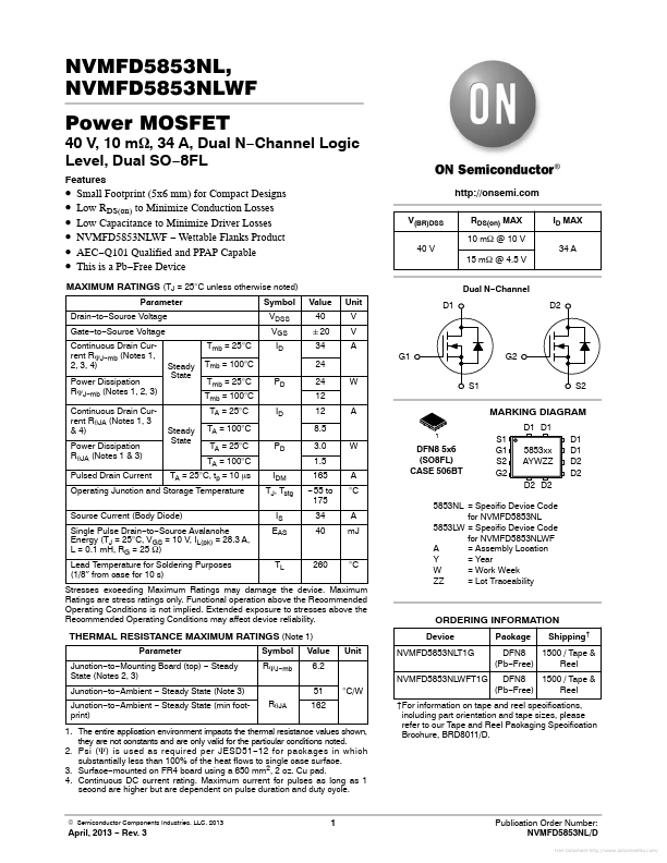
 3) Pulsed Drain Current Tmb = 25°C Steady State Tmb = 100°C Tmb = 25°C Tmb = 100°C TA = 25°C Steady State TA = 100°C TA = 25°C TA = 100°C TA = 25°C, tp = 10 ms IDM TJ, Tstg IS EAS PD ID PD Symbol VDSS VGS ID Value 40 "2