P3P76Z11D Overview
Key Specifications
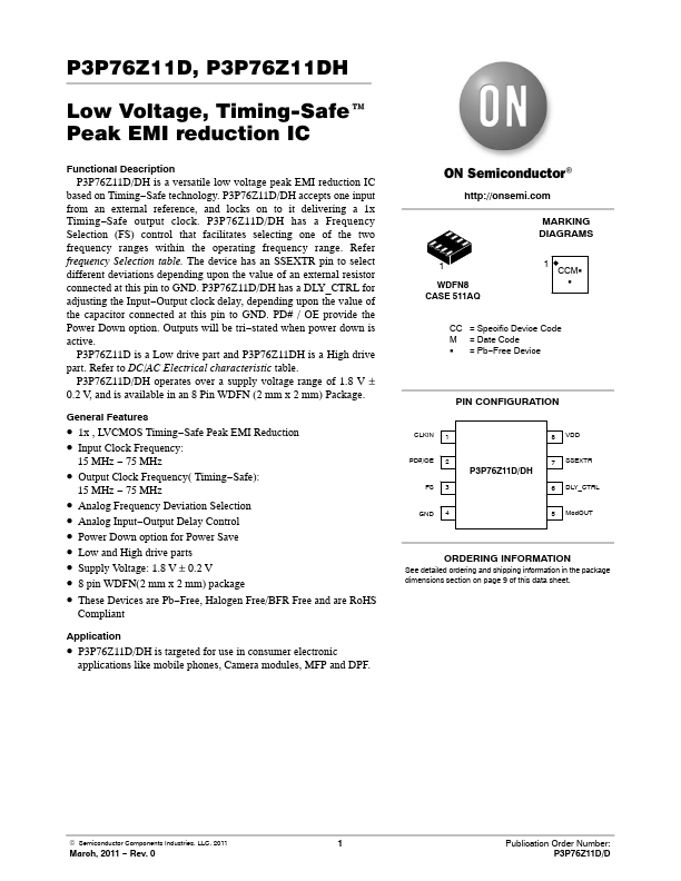
Package: WFDFN
Mount Type: Surface Mount
Pins: 8
Operating Voltage: 1.8 V
Key Features
- 1x , LVCMOS Timing-Safe Peak EMI Reduction
- Input Clock Frequency: 15 MHz
- Output Clock Frequency( Timing-Safe): 15 MHz
- Analog Frequency Deviation Selection
- Analog Input-Output Delay Control