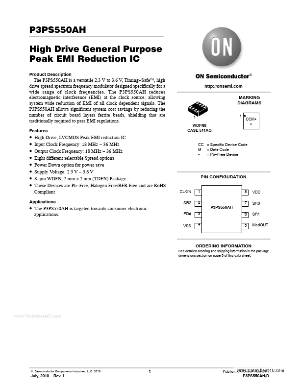
• Part: P3PS550AH
  • Description: High Drive General Purpose Peak EMI Reduction IC
  • Manufacturer: onsemi
  • Size: 135.47 KB
Download P3PS550AH Datasheet PDF
onsemi
P3PS550AH
P3PS550AH is High Drive General Purpose Peak EMI Reduction IC manufactured by onsemi.
Description The P3PS550AH is a versatile 2.3 V to 3.6 V, Timing- Safe™, high drive spread spectrum frequency modulator designed specifically for a wide range of clock frequencies. The P3PS550AH reduces electromagnetic interference (EMI) at the clock source, allowing system wide reduction of EMI of all clock dependent signals. The P3PS550AH allows significant system cost savings by reducing the number of circuit board layers ferrite beads, shielding that are traditionally required to pass EMI regulations. Features http://onsemi. MARKING DIAGRAMS 1 WDFN8 CASE 511AQ 1 CCMG G - - - - - - - - High Drive, LVCMOS Peak EMI reduction IC Input Clock Frequency: 18 MHz - 36 MHz Output Clock Frequency: 18 MHz - 36 MHz Eight different selectable Spread options Power Down option for power save Supply Voltage: 2.3 V - 3.6 V 8- pin WDFN, 2 mm x 2 mm (TDFN) Package These Devices are Pb- Free, Halogen Free/BFR Free and are Ro HS pliant CC = Specific Device Code M = Date Code G = Pb- Free Device PIN CONFIGURATION CLKIN SR2 PD# VSS 1 2 P3PS550AH 3 4 8 7 6 5 VDD SR0 SR1 Mod OUT Applications - The P3PS550AH is targeted towards consumer electronic applications. ORDERING INFORMATION See detailed ordering and shipping information in the package dimensions section on page 5 of this data sheet. .. © Semiconductor ponents Industries, LLC, 2010 July, 2010 - Rev. 1 Publication Order Number: P3PS550AH/D VDD SR0 SR1 SR2 CLKIN Mod OUT PD# Figure 1. Block Diagram P3PS550AH modulates the output of a single PLL in order to “spread” the bandwidth of a synthesized clock, and more importantly, decreases the peak amplitudes of its harmonics. This results in significantly lower system EMI pared to the typical narrow band signal produced by oscillators and most frequency generators. Lowering EMI by increasing a signal’s bandwidth is called ‘spread spectrum clock generation’. Table 1. PIN DESCRIPTION Pin# 1 2 3 Pin Name CLKIN SR2 PD# Type I I I External reference clock...