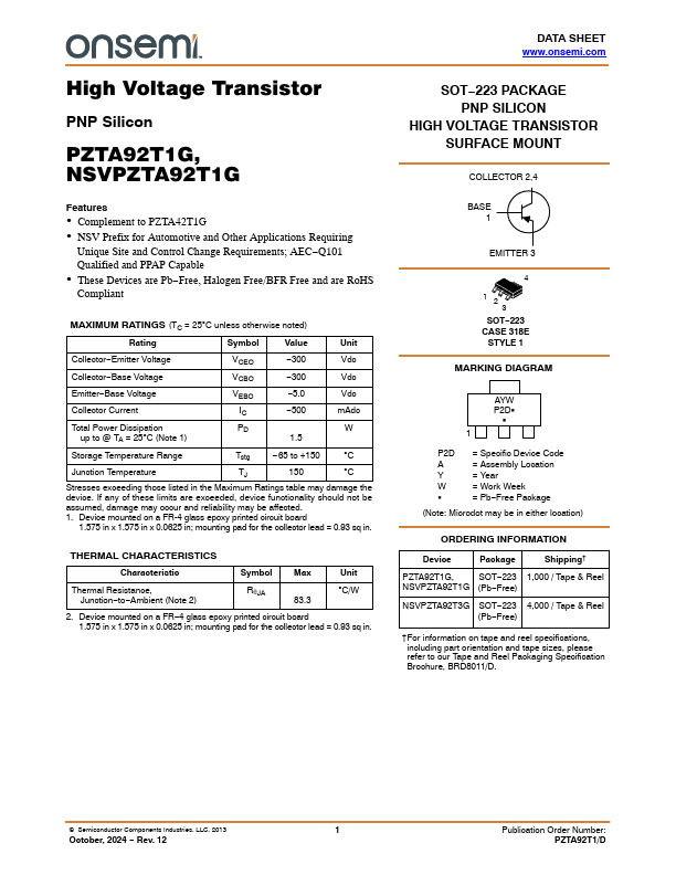
PZTA92T1G
PZTA92T1G is High Voltage PNP Silicon Transistor manufactured by onsemi.
Features
- plement to PZTA42T1G
- NSV Prefix for Automotive and Other Applications Requiring
Unique Site and Control Change Requirements; AEC- Q101
Qualified and PPAP Capable
- These Devices are Pb- Free, Halogen Free/BFR Free and are Ro HS pliant
MAXIMUM RATINGS (TC = 25C unless otherwise noted)
Rating
Symbol
Value
Unit
Collector- Emitter Voltage
VCEO
- 300
Vdc
Collector- Base Voltage
VCBO
- 300
Vdc
Emitter- Base Voltage
VEBO
- 5.0
Vdc
Collector Current
- 500 m Adc
Total Power Dissipation up to @ TA = 25C (Note 1)
Storage Temperature Range
Tstg
- 65 to +150
C
Junction Temperature
C
Stresses exceeding those listed in the Maximum Ratings table may damage the device. If any of these limits are exceeded, device functionality should not be assumed, damage may occur and reliability may be affected. 1. Device mounted on a FR-4 glass epoxy printed circuit board
1.575 in x 1.575 in x 0.0625 in; mounting pad for the collector lead = 0.93 sq in.
THERMAL CHARACTERISTICS
Characteristic...