STD110N02R
STD110N02R is N-Channel Power MOSFET manufactured by onsemi.
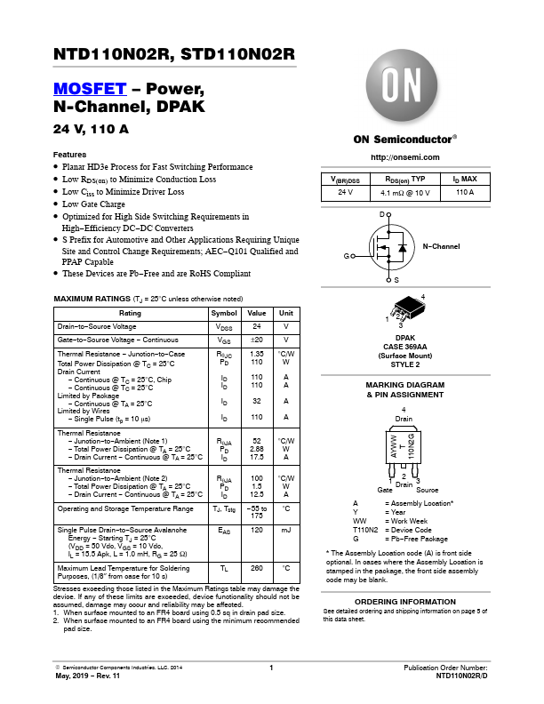
NTD110N02R, STD110N02R
MOSFET
- Power, N-Channel, DPAK
24 V, 110 A
Features
- Planar HD3e Process for Fast Switching Performance
- Low RDS(on) to Minimize Conduction Loss
- Low Ciss to Minimize Driver Loss
- Low Gate Charge
- Optimized for High Side Switching Requirements in
High- Efficiency DC- DC Converters
- S Prefix for Automotive and Other Applications Requiring Unique
Site and Control Change Requirements; AEC- Q101 Qualified and
PPAP Capable
- These Devices are Pb- Free and are Ro HS pliant
MAXIMUM RATINGS (TJ = 25°C unless otherwise noted)
Rating
Symbol Value Unit
Drain- to- Source Voltage
Gate- to- Source Voltage
- Continuous
Thermal Resistance
- Junction- to- Case Total Power Dissipation @ TC = 25°C Drain Current
- Continuous @ TC = 25°C, Chip
- Continuous @ TC = 25°C Limited by Package
- Continuous @ TA = 25°C Limited by Wires
- Single Pulse (tp = 10 ms)
Thermal Resistance
- Junction- to- Ambient (Note 1)
- Total Power Dissipation @ TA =...