TF410
Overview
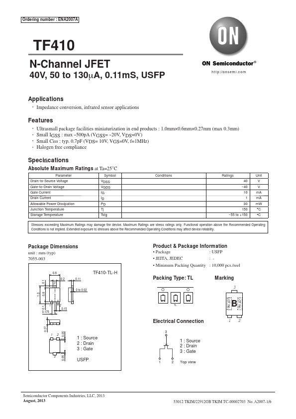
- Ultrasmall package facilities miniaturization in end products : 1.0mm×0.6mm×0.27mm (max 0.3mm)
- Small IGSS : max --500pA (VGSS= --20V, VDS=0V)
- Small Ciss : typ. 0.7pF (VDS= 10V, VGS=0V, f=1MHz)
- Halogen free compliance Specifications