VN2406L
Description
VN2406L Preferred Device Small Signal MOSFET 200 mAmps, 240 Volts N−Channel TO−92 MAXIMUM RATINGS Rating Drain −Source Voltage Drain −Gate Voltage Gate −Source Voltage − Continuous − Non−repetitive (...
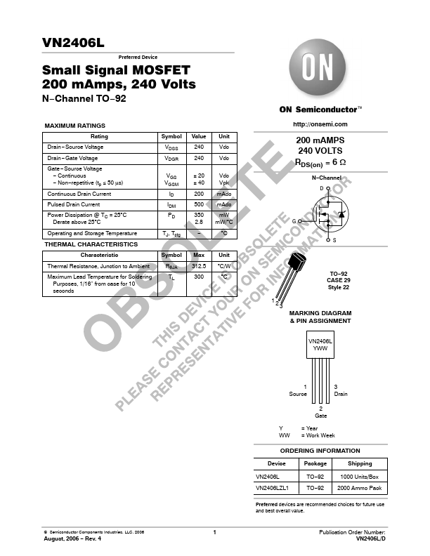
VN2406L Preferred Device Small Signal MOSFET 200 mAmps, 240 Volts N−Channel TO−92 MAXIMUM RATINGS Rating Drain −Source Voltage Drain −Gate Voltage Gate −Source Voltage − Continuous − Non−repetitive (...
| Part Number | Manufacturer | Description |
|---|---|---|
| VN2406 | Supertex Inc | N-Channel Vertical DMOS FETs |
| VN2406B | Siliconix | N-Channel Enhancement-Mode MOS Transistors |
| VN2406D | Siliconix | N-Channel Enhancement-Mode MOS Transistors |