NTB85N03T4
NTB85N03T4 is Power MOSFET manufactured by onsemi.
NTP85N03, NTB85N03 Power MOSFET 85 Amps, 28 Volts
N- Channel TO- 220 and D2PAK
Designed for low voltage, high speed switching applications in power supplies, converters and power motor controls and bridge circuits.
Typical Applications http://onsemi.
- -
- -
Power Supplies Converters Power Motor Controls Bridge Circuits
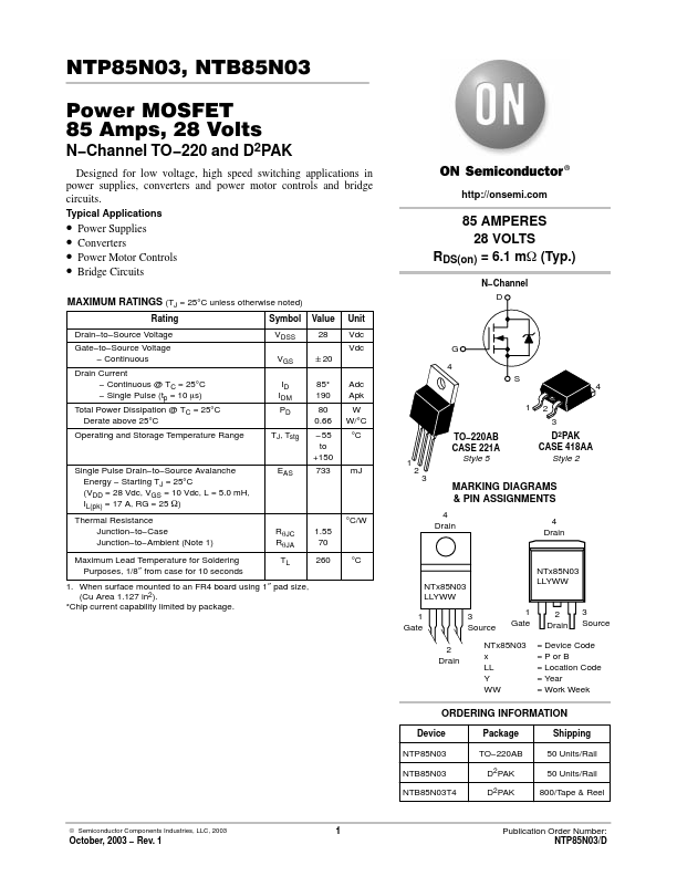
85 AMPERES 28 VOLTS RDS(on) = 6.1 m W (Typ.)
N- Channel D Value 28 "20 85- 190 80 0.66
- 55 to +150 733 Adc Apk W W/°C °C 1 TO- 220AB CASE 221A Style 5 2 3 Unit Vdc Vdc VGS ID IDM PD TJ, Tstg G 4 S 1 2 3 D2PAK CASE 418AA Style 2 4
MAXIMUM RATINGS (TJ = 25°C unless otherwise noted)
Rating Drain- to- Source Voltage Gate- to- Source Voltage
- Continuous Drain Current
- Continuous @ TC = 25°C
- Single Pulse (tp = 10 ms) Total Power Dissipation @ TC = 25°C Derate above 25°C Operating and Storage Temperature Range Symbol VDSS
Single Pulse Drain- to- Source Avalanche Energy
- Starting TJ = 25°C (VDD = 28 Vdc, VGS = 10 Vdc, L = 5.0 m H, IL(pk) = 17 A, RG = 25 W) Thermal Resistance Junction- to- Case Junction- to- Ambient (Note 1) Maximum Lead Temperature for Soldering Purposes, 1/8″ from case for 10 seconds
EAS m J
MARKING DIAGRAMS & PIN ASSIGNMENTS
°C/W Rq JC Rq JA TL 1.55 70 260 °C NTx85N03 LLYWW 1 Gate 2 Drain 3 Source 1 Gate NTx85N03 LLYWW 4 Drain 4 Drain
1. When surface mounted to an FR4 board using 1″ pad size, (Cu Area 1.127 in2).
- Chip current capability limited by package.
2 Drain
3 Source
NTx85N03 x LL Y WW
= Device Code = P or B = Location Code = Year = Work Week
ORDERING INFORMATION
Device NTP85N03 NTB85N03 NTB85N03T4 Package TO- 220AB D2PAK D2PAK Shipping 50 Units/Rail 50 Units/Rail 800/Tape & Reel
© Semiconductor ponents Industries, LLC, 2003
October, 2003
- Rev. 1
Publication Order Number: NTP85N03/D
NTP85N03, NTB85N03
ELECTRICAL CHARACTERISTICS (TJ = 25°C unless otherwise noted)
Characteristic OFF CHARACTERISTICS Drain- to- Source Breakdown Voltage (Note 2) (VGS = 0 Vdc, ID = 250 m Adc) Temperature Coefficient (Positive) Zero Gate Voltage...