ESD11N5.0ST5G Description
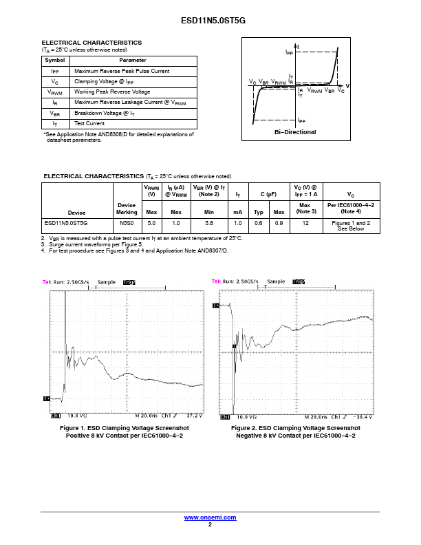
© Semiconductor ponents Industries, LLC, 2010 1 November, 2017 − Rev. 5 Publication Order Number: ESD11N5.0S/D ESD11N5.0ST5G (TA = 25°C unless otherwise noted) Symbol Parameter IPP Maximum Reverse Peak Pulse Current VC Clamping Voltage @ IPP VRWM Working Peak Reverse Voltage IR Maximum Reverse Leakage Current @ VRWM VBR Breakdown Voltage @ IT IT Test Current See Application Note AND8308/D for detailed explanations...
ESD11N5.0ST5G Key Features
- Low Capacitance 0.6 pF
- Low Clamping Voltage
- Small Body Outline Dimensions: 0.60 mm x 0.30 mm
- Low Body Height: 0.3 mm
- Stand-off Voltage: 5.0 V
- Low Leakage
- Response Time is < 1 ns
- IEC61000-4-2 Level 4 ESD Protection
- These Devices are Pb-Free, Halogen Free/BFR Free and are RoHS
- Maximum (10 Second Duration)