FDC638APZ Description
This P−Channel 2.5 V specified MOSFET is produced using onsemi’s advanced POWERTRENCH process that has been especially tailored to minimize the on−state resistance and yet maintain low gate charge for superior switching performance. These devices are well suited for battery power applications: load switching and power management, battery charging circuits, and DC/DC conversion.
FDC638APZ Key Features
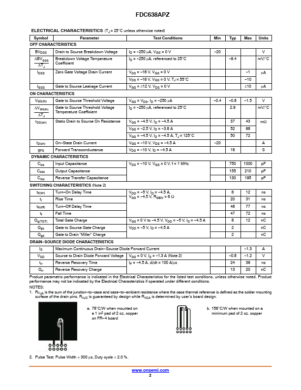
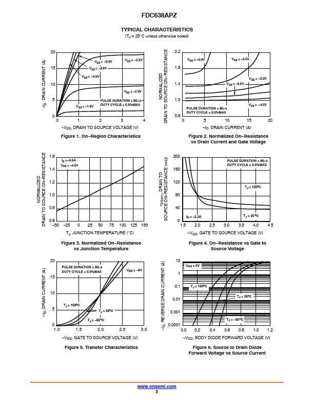
- Max rDS(on) = 43 mW at VGS = -4.5 V, ID = -4.5 A
- Max rDS(on) = 68 mW at VGS = -2.5 V, ID = -3.8 A
- Low Gate Charge (8 nC typical)
- High Performance Trench Technology for Extremely Low rDS(on)
- SUPERSOTt-6 Package: Small Footprint (72% smaller than
- This Device is Pb-Free, Halide Free and is RoHS pliant
- DC-DC Conversion
- 55 to +150 °C
- Rev. 3
- 20 -9.4