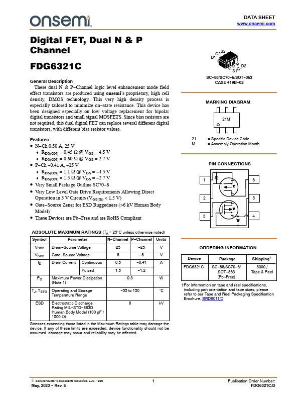
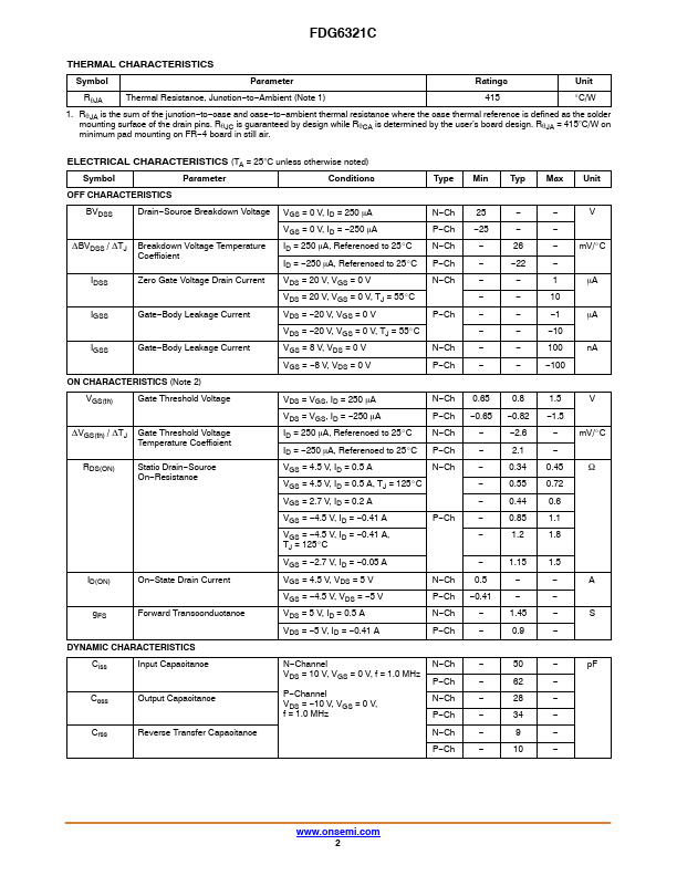
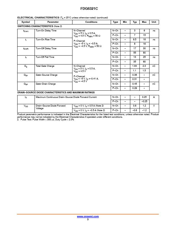
FDG6321C Description
These dual N & P−Channel logic level enhancement mode field effect transistors are produced using onsemi’s proprietary, high cell density, DMOS technology. This very high density process is especially tailored to minimize on−state resistance. This device has been designed especially on low voltage replacement for bipolar digital transistors and small signal MOSFETS.
FDG6321C Key Features
- N-Ch 0.50 A, 25 V
- RDS(ON) = 0.45 W @ VGS = 4.5 V
- RDS(ON) = 0.60 W @ VGS = 2.7 V
- P-Ch -0.41 A, -25 V
- RDS(ON) = 1.1 W @ VGS = -4.5 V
- RDS(ON) = 1.5 W @ VGS = -2.7 V
- Very Small Package Outline SC70-6
- Very Low Level Gate Drive Requirements Allowing Direct
- Gate-Source Zener for ESD Ruggedness (>6 kV Human Body
- These Devices are Pb-Free and are RoHS pliant