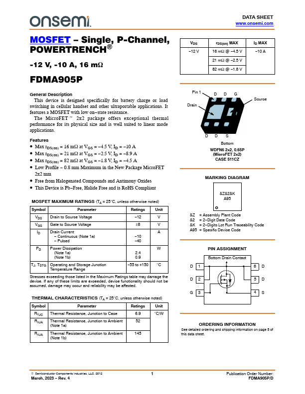
FDMA905P Overview
Description
This device is designed specifically for battery charge or load switching in cellular handset and other ultraportable applications. It features a MOSFET with low on-state resistance.
Key Features
- Max rDS(on) = 16 mW at VGS = -4.5 V, ID = -10 A
- Max rDS(on) = 21 mW at VGS = -2.5 V, ID = -8.9 A
- Max rDS(on) = 82 mW at VGS = -1.8 V, ID = -4.5 A
- 0.8 mm Maximum in the New Package MicroFET 2x2 mm
- Free from Halogenated Compounds and Antimony Oxides
- Continuous (Note 1a)
- 12 V ±8 V A -10 -40 PD Power Dissipation (Note 1a) (Note 1b) W 2.4 0.9 TJ, TSTG Operating and Storage Junction Temperature Range