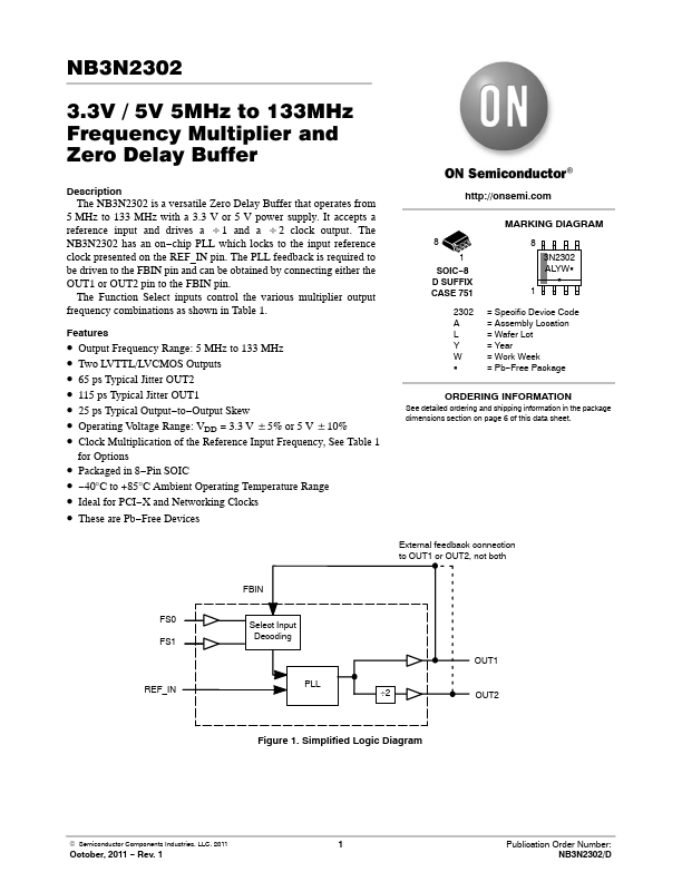
NB3N2302 Description
The NB3N2302 is a versatile Zero Delay Buffer that operates from 5 MHz to 133 MHz with a 3.3 V or 5 V power supply. It accepts a reference input and drives a B1 and a B2 clock output. The NB3N2302 has an on−chip PLL which locks to the input reference clock presented on the REF_IN pin.
NB3N2302 Key Features
- Output Frequency Range: 5 MHz to 133 MHz
- Two LVTTL/LVCMOS Outputs
- 65 ps Typical Jitter OUT2
- 115 ps Typical Jitter OUT1
- 25 ps Typical Output-to-Output Skew
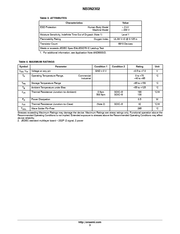
- Operating Voltage Range: VDD = 3.3 V $5% or 5 V $10%
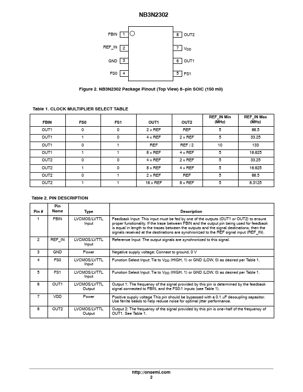
- Clock Multiplication of the Reference Input Frequency, See Table 1
- Packaged in 8-Pin SOIC
- 40°C to +85°C Ambient Operating Temperature Range
- Ideal for PCI-X and Networking Clocks