NB3N106K
NB3N106K is 3.3V Differential 1:6 Fanout Clock Driver manufactured by onsemi.
3.3V Differential 1:6 Fanout
Clock Driver with HCSL
Outputs
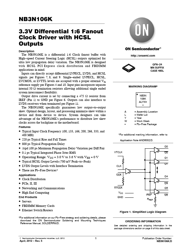
Description The NB3N106K is a differential 1:6 Clock fanout buffer with
High- speed Current Steering Logic (HCSL) outputs optimized for ultra low propagation delay variation. The NB3N106K is designed with HCSL PCI Express clock distribution and FBDIMM applications in mind.
Inputs can directly accept differential LVPECL, LVDS, and HCSL signals per Figures 7, 8, and 9. Single- ended LVPECL, HCSL, LVCMOS, or LVTTL levels are accepted with a proper external Vth reference supply per Figures 4 and 10. Input pins incorporate separate internal 50 W termination resistors allowing additional single ended system interconnect flexibility.
Output drive current is set by connecting a 475 W resistor from IREF (Pin 1) to GND per Figure 6. Outputs can also interface to LVDS receivers when terminated per Figure 11.
The NB3N106K specifically guarantees low output- to- output skew. Optimal design, layout, and processing minimize skew within a device and from device to device. System designers can take advantage of the NB3N106K’s performance to distribute low skew clocks across the backplane or the motherboard.
Features
- Typical Input Clock Frequency 100, 133, 166, 200, 266, 333, and
400 MHz
- 220 ps Typical Rise and Fall Times
- 800 ps Typical Propagation Delay
- Dtpd 100 ps Maximum Propagation Delay Variation per Diff Pair
- 0.1 ps Typical Integrated Phase Jitter RMS
- Operating Range: VCC = 3.0 V to 3.6 V with VEE = 0 V
- Typical HCSL Output Levels (700 m V Peak- to- Peak)
- LVDS Output Levels with Interface Termination
- These are Pb- Free Devices-
Applications
- Clock Distribution
- PCIe, II, III
- Networking and munications
- High End puting
End Products
- Servers
- FBDIMM Memory Cards
- Ethernet Switch/Routers
- For additional information on our Pb- Free strategy and soldering details, please download the ON Semiconductor Soldering and Mounting Techniques Reference Manual, SOLDERRM/D. http://onsemi.
QFN- 24...