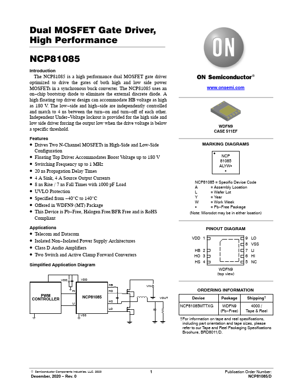
NCP81085 Description
Pin No. DFN9 Symbol 1 VDD 2 HB 3 HO 4 HS 5 NC 6 HI 7 LI 8 VSS 9 LO Description Positive Supply to the Lower Gate Driver High Side Bootstrap Supply High Side Output High−Side Source No Connect High−Side Input Low−Side Input Negative Supply Return Low Side.
NCP81085 Key Features
- Drives Two N-Channel MOSFETs in High-Side and Low-Side
- Floating Top Driver Acmodates Boost Voltage up to 180 V
- Switching Frequency up to 1 MHz
- 20 ns Propagation Delay Times
- 4 A Sink, 4 A Source Output Currents
- 8 ns Rise / 7 ns Fall Times with 1000 pF Load
- UVLO Protection
- Specified from -40°C to 140°C
- Offered in WDFN9 (MT) Package
- This Device is Pb-Free, Halogen Free/BFR Free and is RoHS