NCV59801 Description
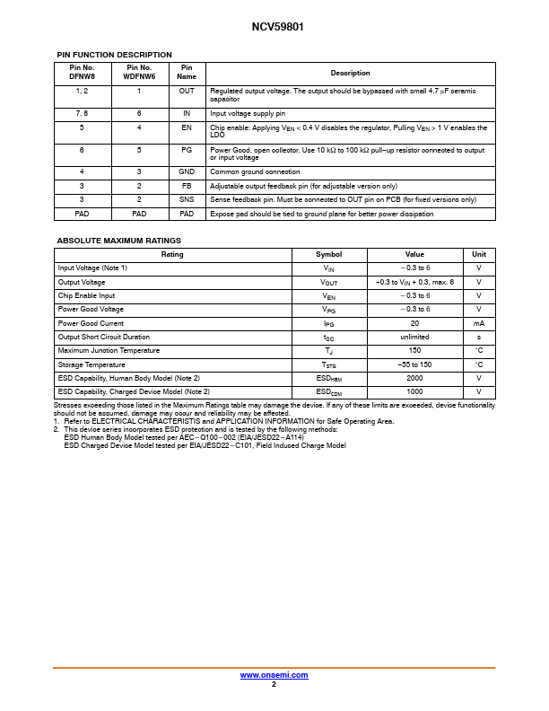
The output should be bypassed with small 4.7 mF ceramic capacitor Input voltage supply pin Chip enable: Applying VEN < 0.4 V disables the regulator, Pulling VEN > 1 V enables the LDO Power Good, open collector. Use 10 kW to 100 kW pull−up resistor connected to output or input voltage mon ground connection Adjustable output feedback pin (for adjustable version only) Sense feedback pin.
NCV59801 Key Features
- Operating Input Voltage Range: 1.6 V to 5.5 V
- Available in Fixed Voltage Option: 0.6 V to 5.0 V
- Adjustable Version Reference Voltage: 0.6 V
- ±0.7% Initial Accuracy at 25°C
- ±1% Accuracy Over Load and Temperature (up to 125°C)
- Low Quiescent Current Typ. 35 mA
- Shutdown Current: Typ. 0.1 mA
- Very Low Dropout: Typ. 120 mV at 1 A for 3.3 V Variant
- High PSRR: Typ. 85 dB at 100 mA, f = 1 kHz
- Low Noise: 10 mVRMS (Fixed Version)