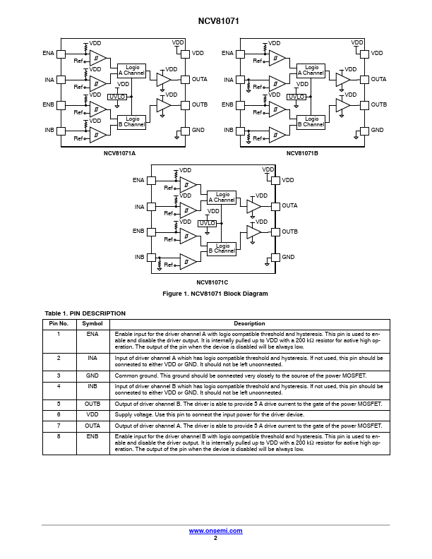
NCV81071 Description
Symbol Description 1 ENA Enable input for the driver channel A with logic patible threshold and hysteresis. This pin is used to en- able and disable the driver output. It is internally pulled up to VDD with a 200 kW resistor for active high op- eration.
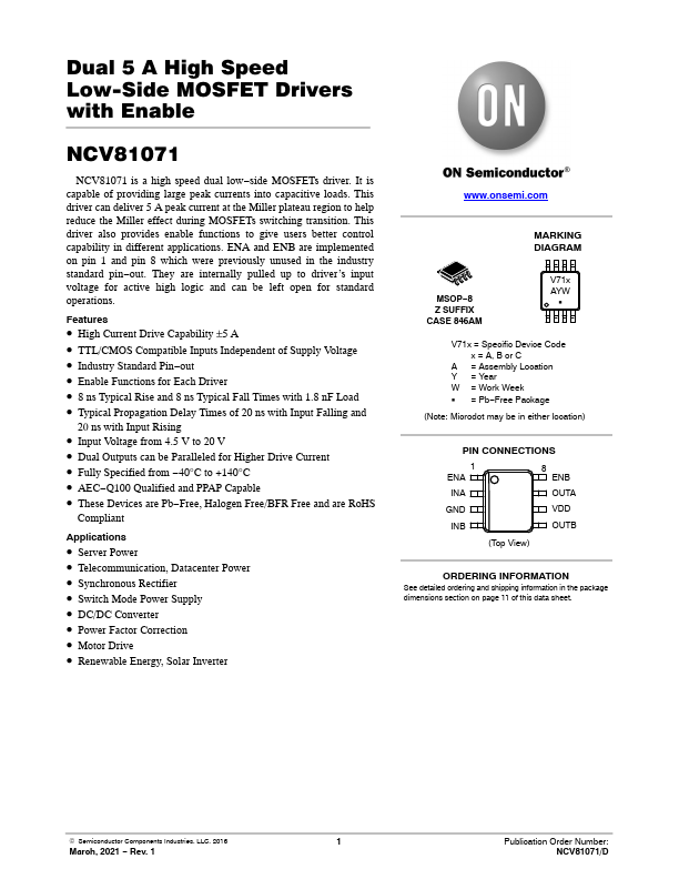
NCV81071 Key Features
- High Current Drive Capability ±5 A
- TTL/CMOS patible Inputs Independent of Supply Voltage
- Industry Standard Pin-out
- Enable Functions for Each Driver
- 8 ns Typical Rise and 8 ns Typical Fall Times with 1.8 nF Load
- Typical Propagation Delay Times of 20 ns with Input Falling and
- Input Voltage from 4.5 V to 20 V
- Dual Outputs can be Paralleled for Higher Drive Current
- Fully Specified from -40°C to +140°C
- AEC-Q100 Qualified and PPAP Capable