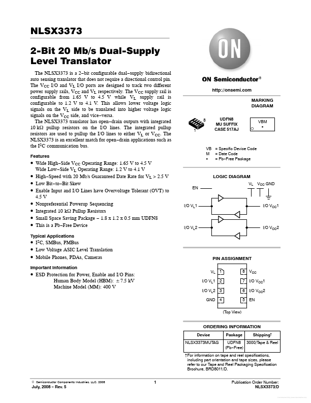
NLSX3373 Description
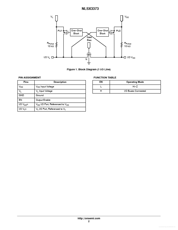
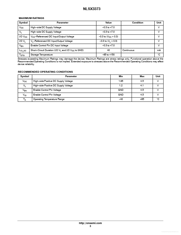
VCC Input Voltage VL Input Voltage Ground Output Enable VCC I/O Port, Referenced to VCC VL I/O Port, Referenced to VL FUNCTION TABLE EN L H Operating Mode Hi−Z I/O Buses Connected http://onsemi. 2 Free Datasheet http://../ NLSX3373 MAXIMUM RATINGS Symbol VCC VL I/O VCC I/O VL VEN II/O_SC TSTG Parameter High−side DC Supply Voltage High−side DC Supply Voltage VCC−Referenced DC Input/Output Voltage VL−Referenced DC...
NLSX3373 Key Features
- Wide High-Side VCC Operating Range: 1.65 V to 4.5 V
- High-Speed with 20 Mb/s Guaranteed Date Rate for VL > 2.5 V
- Low Bit-to-Bit Skew
- 1.8 x 1.2 x 0.5 mm UDFN8 This is a Pb-Free Device Wide Low-Side VL Operating Range: 1.2 V to 4.1 V
NLSX3373 Applications
- Wide High−Side VCC Operating Range: 1.65 V to 4.5 V
- High−Speed with 20 Mb/s Guaranteed Date Rate for VL > 2.5 V
- Low Bit−to−Bit Skew
- Enable Input and I/O Lines have Overvoltage Tolerant (OVT) to