NUP4012PXV6 Description
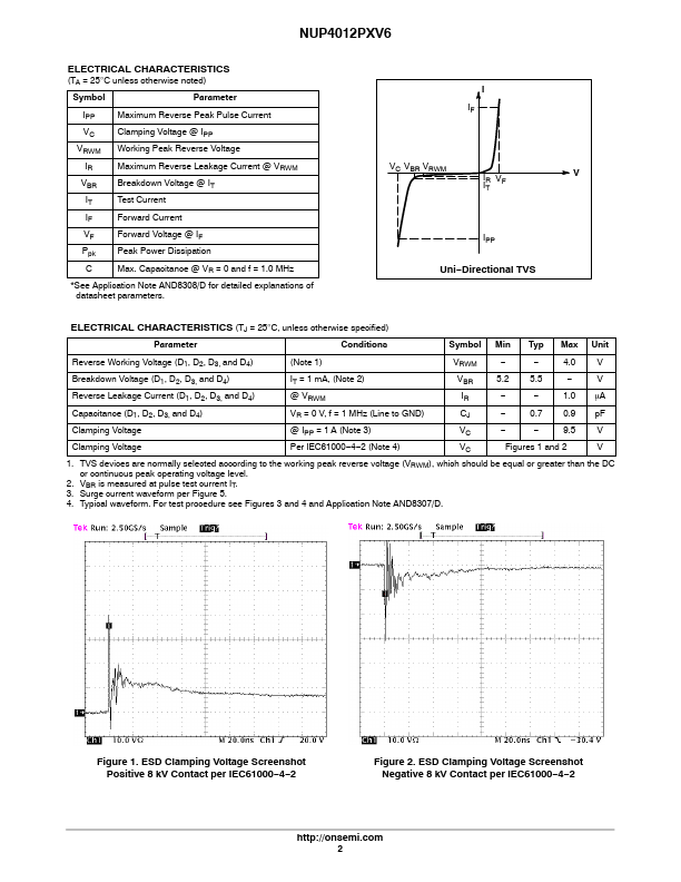
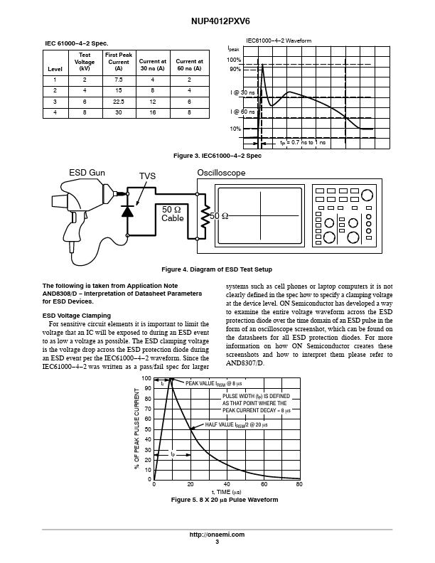
© Semiconductor ponents Industries, LLC, 2009 1 August, 2009− Rev. 1 Publication Order Number: NUP4012PXV6/D NUP4012PXV6 (TA = 25°C unless otherwise noted) Symbol Parameter IPP Maximum Reverse Peak Pulse Current VC Clamping Voltage @ IPP VRWM Working Peak Reverse Voltage IR Maximum Reverse Leakage Current @ VRWM VBR Breakdown Voltage @ IT IT Test Current IF Forward Current VF Forward Voltage @ IF Ppk Peak Power...
NUP4012PXV6 Key Features
- Low Capacitance (0.7 pF Typical)
- Protects up to Four Data Lines
- SOT-563 1.6 mm x 1.6 mm
- Low Profile of 0.55 mm for Slim Design Ultra
- D1, D2, D3, and D4 Pins = 5.2 V Minimum Protection
- ESD Rating: IEC61000-4-2: Level 4
- This is a Pb-Free Device