NVMFS5A140PLZ Overview
Key Features
- Small Footprint (5 x 6 mm) for Compact Design
- Low RDS(on) to Minimize Conduction Losses
- NVMFS5A140PLZWF: Wettable Flank Option for Enhanced Optical Inspection
- AEC-Q101 Qualified and PPAP Capable
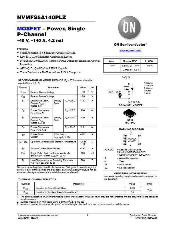
- 40 ±20 -140 V V A D (5) G (4) 1: Source 2: Source 3: Source 4: Gate 5: Drain S (1,2,3) P-CHANNEL MOSFET PD Power Dissipation RqJC (Note
- TC = 25°C 200 ID Continuous Drain: Steady TA = 25°C
- 20 C(Nuorrteesnt1R, 2qJ,A3) State W A DFN5 (SO-8FL) PD Power Dissipation RqJA (Note 1
- TA = 25°C 3.8 W IDP Pulsed Drain Current PW ≤ 10 ms, duty cycle ≤ 1%
- 560 A TJ, TSTG Operating Junction and Storage Temperature