PJQ1821
PJQ1821 is 20V P-Channel Enhancement Mode MOSFET manufactured by PanJit Semiconductor.
Features
- Advanced Trench Process Technology
- Specially Designed for Switch Load, PWM Application, etc.
- ESD Protected
- Lead free in pliance with EU Ro HS 2.0
- Green molding pound as per IEC 61249 standard
Mechanical Data
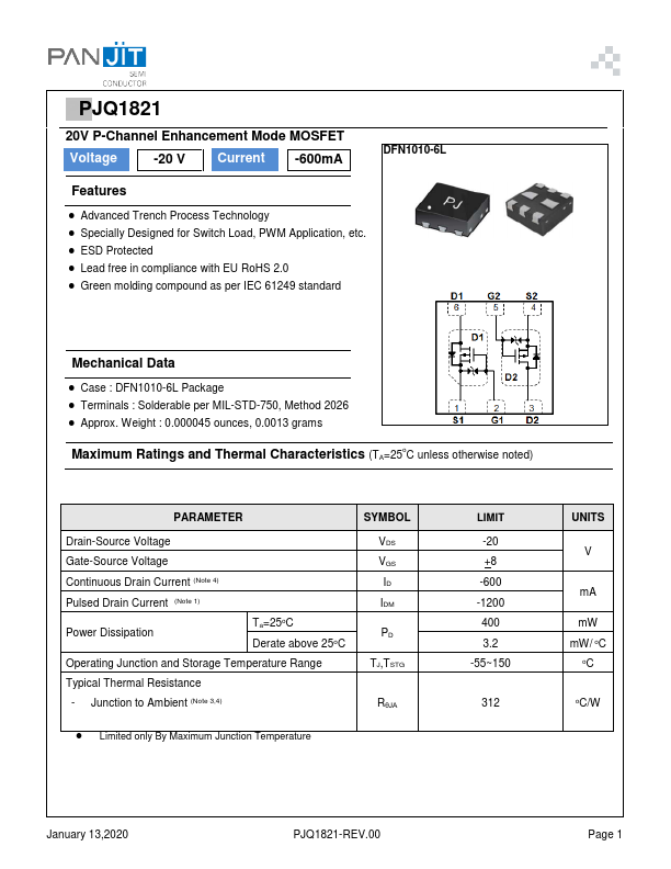
- Case : DFN1010-6L Package
- Terminals : Solderable per MIL-STD-750, Method 2026
- Approx. Weight : 0.000045 ounces, 0.0013 grams
Maximum Ratings and Thermal Characteristics (TA=25o C unless otherwise noted)
PARAMETER
Drain-Source Voltage
Gate-Source Voltage
Continuous Drain Current (Note 4)
Pulsed Drain Current (Note 1)
Power Dissipation
Ta=25o C Derate above 25o C
Operating Junction and Storage Temperature Range
Typical Thermal Resistance
- Junction to Ambient (Note 3,4)
SYMBOL VDS VGS ID IDM PD
TJ,TSTG
RθJA
- Limited only By Maximum Junction Temperature
LIMIT -20 +8 -600
-1200 400 3.2 -55~150
UNITS V m A m W m W/ o C o C o C/W
January 13,2020
PJQ1821-REV.00
Page 1
PPJQ1821
Electrical Characteristics (TA=25o C unless otherwise noted)
PARAMETER Static Drain-Source Breakdown Voltage Gate Threshold Voltage
Drain-Source On-State Resistance
Zero Gate Voltage Drain Current Gate-Source Leakage Current Dynamic (Note 5) Total Gate Charge Gate-Source Charge Gate-Drain Charge Input Capacitance Output Capacitance Reverse Transfer Capacitance Turn-On Delay Time Turn-On Rise Time Turn-Off Delay Time Turn-Off Fall Time Drain-Source Diode Maximum Continuous Drain-Source Diode Forward Current
SYMBOL
BVDSS VGS(th)
RDS(on)...