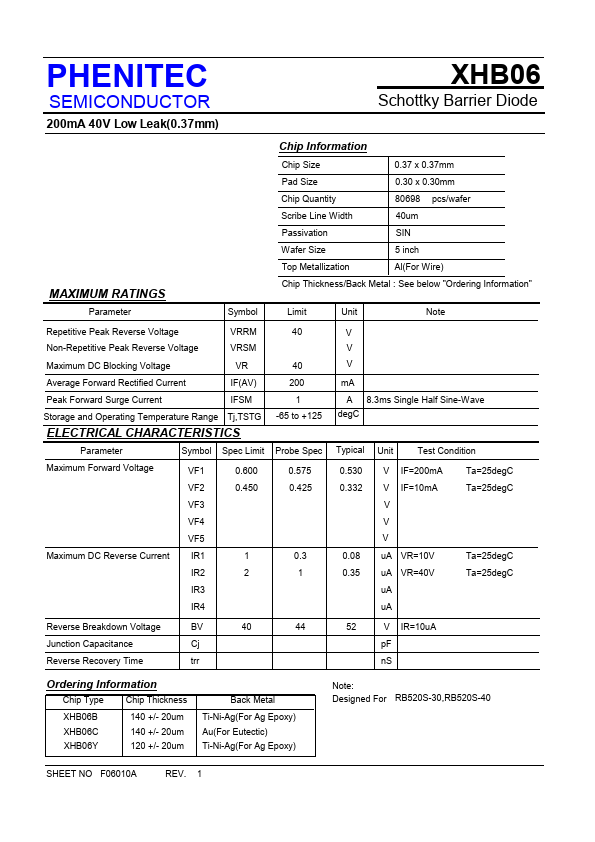
Parameter Symbol Chip Size 0.37 x 0.37mm Pad Size 0.30 x 0.30mm Chip Quantity 80698 pcs/wafer Scribe Line Width 40um Passivation SIN Wafer Size 5 inch Top Metallization Al(For Wire) Chip Thickness/Back Metal : See below "Ordering Information" Limit Unit Note Repetitive Peak Reverse Voltage VRRM 40 Non-Repetitive Peak Reverse Voltage VRSM Maximum DC Blocking Voltage VR 40 Average Forward Rectified Current IF(AV) 200 Peak Forward Surge Current IFSM Storage and Operating Temperature Range Tj,TSTG
ELECTRICAL CHARACTERISTICS
1 -65 to +125 Parameter Symbol Spec Limit Probe Spec Maximum Forward Voltage VF1 0.600 0.575 VF2 0.450 0.425 VF3 VF4 VF5 Maximum DC Reverse Current IR1 1 0.3 IR2 2 1 IR3 IR4 V V V mA A 8.3ms Single Half Sine-Wave degC Typical Unit Test Condition 0.530 0.332 0.08 0.35 V IF=200mA V IF=10mA V V V uA VR=10V u
This website uses cookies or similar technologies, to enhance your browsing experience and provide personalized recommendations. By continuing to use our website, you agree to our Privacy Policy