PSD PAP3050
-30V P-channel enhancement mode MOSFET
| Part No. | PAP3050 |
|---|---|
| Datasheet | PAP3050 Download |
| Manufacturer | PSD |
| Description | -30V P-channel enhancement mode MOSFET |
| Buy | Stock & Price |
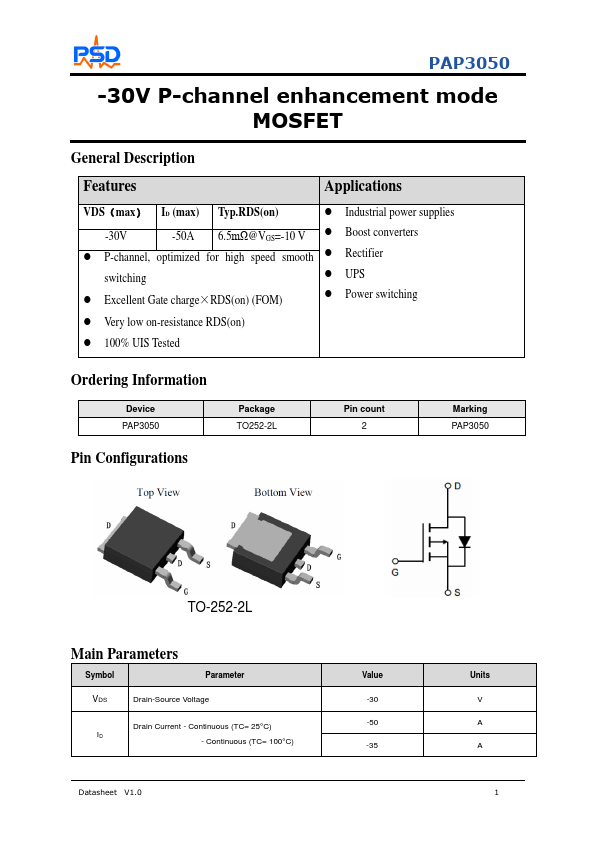
GENERAL DESCRIPTION
FEATURES
APPLICATIONS
VDS(max) ID (max) Typ.RDS(on)● Industrial power supplies -30V -50A 6.5mΩ@VGS=-10 V
● Boost converters
● P-channel, optimized for high speed smooth
● Rectifier switching
● UPS
● Excellent Gate charge×RDS(on) (FOM)
● Power switching
● Very low on-resistance RDS(on)
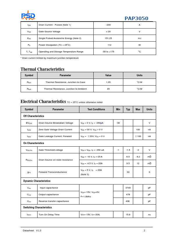
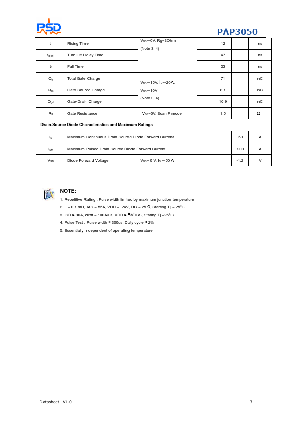
● 100% UIS Tested Ordering Information Device PAP3050 Pin Configurations Package TO252-2L Pin count 2 Marking PAP3050 TO-252-2L Main Parameters Symbol Parameter VDS Drain-Source Voltage Drain Current - Continuous (TC= 25°C) ID - Continuous (TC= 100°C) Datasheet V1.0 Value -30 -50 -35 Units V A A 1 IDM Drain Current - Pulsed (Note 1) VGS Gate-Source Voltage EAS Single Pulsed Avalanche Energy (Note 2) PD Power Dissipation (TC = 25°C) Tj ,Tstg Operating and Storage Temperature Range * Drain current limited by maximum junction temperature Thermal Characteristics Symbol Parameter RθJC Thermal Resistance, Junction-to-Case RθJA Thermal Resistance, Junction-to-Ambient -200 ± 20 151.25 112 -55...