FEATURES
Full CMOS, 6T Cell High Speed (Equal Access and Cycle Times) – 15/20/25/35 ns (Commercial/Industrial) – 15/20/25/35/45 ns (Military) Low Power Operation Single 5V±10% Power Supply Output Enable (OE) & Chip Enable (CE1 and CE2) Control Functions P4C1299/P4C1299L ULTRA HIGH SPEED 64K x 4 STATIC CMOS RAM Data Retention with 2.0V Supply (P4C1299L) Three-State Outputs TTL/CMOS Compatible Outputs Fully TTL Compatible Inputs Standard Pinout (JEDEC Approved) – 28-Pin 300 mil DIP, SOJ – 28-Pin 350x550 mil LCC DESCRIPTION
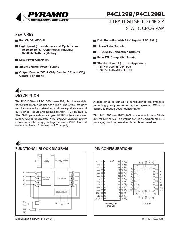
Inputs and outputs are fully TTL-compatible. Current drain is typically 10 µA from a 2.0V supply. Access times as fast as 15 nanoseconds are available, permitting greatly enhanced system speeds. CMOS is utilized to reduce power consumption. The P4C1299 and P4C1299L are available in a 28-pin 300 mil DIP or SOJ, as well as a 28-pin 350x550 mil LCC package, providing excellent board level densities. Functional Block Diagram Pin ConfigurationS Document # SRAM144 REV OR DIP... PYRAMID