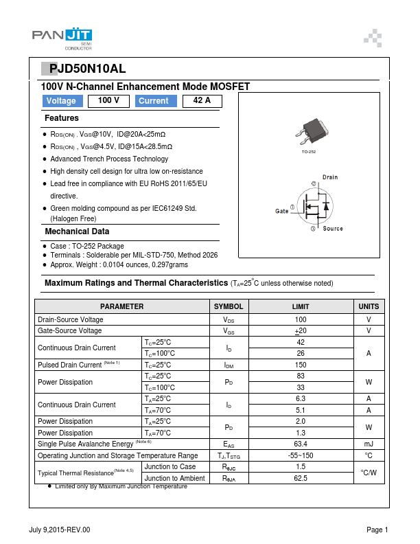
PJD50N10AL Overview
Key Specifications
Max Operating Temp: 150 °C
Min Operating Temp: -55 °C
Key Features
- RDS(ON) , VGS@10V, ID@20A<25mΩ
- RDS(ON) , VGS@4.5V, ID@15A<28.5mΩ
- Advanced Trench Process Technology
- High density cell design for ultra low on-resistance
- Lead free in compliance with EU RoHS 2011/65/EU directive