2SC5216
Overview
- 65±0.15
- 5 -0.05 +0.25
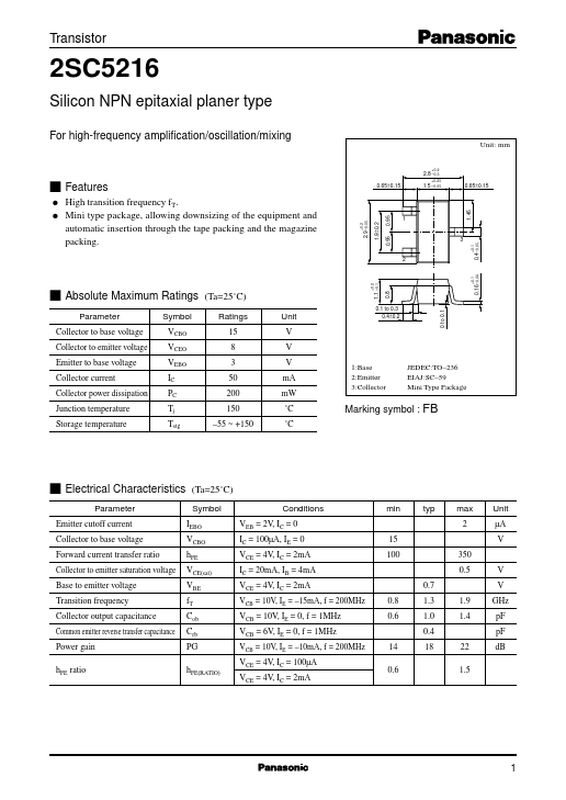
- 65±0.15 2 s Absolute Maximum Ratings Parameter Collector to base voltage Collector to emitter voltage Emitter to base voltage Collector current Collector power dissipation Junction temperature Storage temperature Symbol VCBO VCEO VEBO IC PC Tj Tstg +0.2 1.1 -0.1 (Ta=25˚C) Ratings 15 8 3 50 200 150 -55 ~ +150 Unit V V V mA mW ˚C ˚C 1:Base 2:Emitter 3:Collector JEDEC:TO-236 EIAJ:SC-59 Mini Type Package Marking symbol : FB s Electrical Characteristics Parameter Emitter cutoff current Collector to base voltage Forward current transfer ratio Collector to emitter saturation voltage Base to emitter voltage Transition frequency Collector output capacitance Common emitter reverse transfer capacitance Power gain hFE ratio (Ta=25˚C) Symbol IEBO VCBO hFE VCE(sat) VBE fT Cob Crb PG hFE(RATIO) Conditions VEB = 2V, IC = 0 IC = 100µA, IE = 0 VCE = 4V, IC = 2mA IC = 20mA, IB = 4mA VCE = 4V, IC = 2mA VCB = 10V, IE = -15mA, f = 200MHz VCB = 10V, IE = 0, f = 1MHz VCB = 6V, IE = 0, f = 1MHz VCB = 10V, IE = -10mA, f = 200MHz VCE = 4V, IC = 100µA VCE = 4V, IC = 2mA 14 0.6 0.8 0.6 0.7 1.3 1.0 0.4 18 22 1.5 1.9 1.4 15 100 350 0.5 V V GHz pF pF dB min typ max 2 Unit µA V 0 to 0.1
- 1 to 0.3 0.4±0.2
- 16 -0.06 +0.1
- 4 -0.05 +0.1 High transition frequency fT. Mini type package, allowing downsizing of the equipment and automatic insertion through the tape packing and the magazine packing.
- 9 -0.05 1
- 9±0.2 +0.2
- 45 1 Transistor PC - Ta 250 120 Ta=25˚C 100 100 2SC5216 IC - VCE 120 VCE=4V IC - VBE Collector power dissipation PC (mW) Collector current IC (mA) 80 IB=600µA 60 500µA 400µA 300µA 200µA 20 100µA Collector current IC (mA) 200 80 150 60 25˚C 40 100 40 Ta=75˚C -25˚C 50 20