2SC5243
Overview
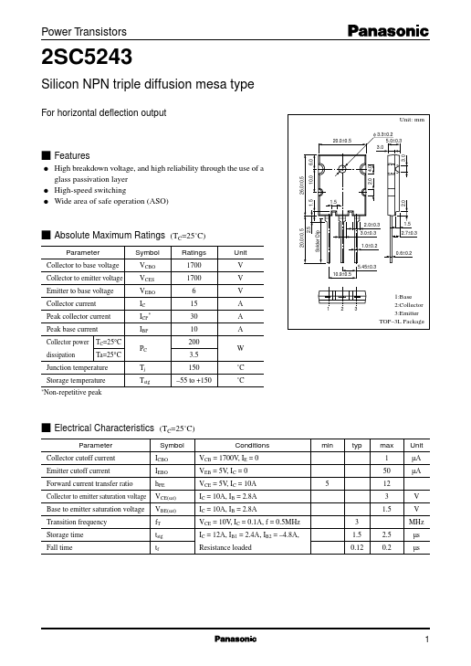
- 5 Solder Dip s Absolute Maximum Ratings Parameter Collector to base voltage Collector to emitter voltage Emitter to base voltage Collector current Peak collector current Peak base current Collector power TC=25°C dissipation Ta=25°C Junction temperature Storage temperature
- Non-repetitive
- 0±0.5 2.5
- 0±0.3 3.0±0.3 1.0±0.2 (TC=25˚C) Ratings 1700 1700 6 15 30 10 200 3.5 150 -55 to +150 Unit V V V A A A W ˚C ˚C
- 7±0.3 Symbol VCBO VCES VEBO IC ICP* IBP PC Tj Tstg
- 6±0.2 5.45±0.3 10.9±0.5 1 2 3 1:Base 2:Collector 3:Emitter TOP-3L Package peak s Electrical Characteristics Parameter Collector cutoff current Emitter cutoff current Forward current transfer ratio Collector to emitter saturation voltage Base to emitter saturation voltage Transition frequency Storage time Fall time (TC=25˚C) Symbol ICBO IEBO hFE VCE(sat) VBE(sat) fT tstg tf Conditions VCB = 1700V, IE = 0 VEB = 5V, IC = 0 VCE = 5V, IC = 10A IC = 10A, IB = 2.8A IC = 10A, IB = 2.8A VCE = 10V, IC = 0.1A, f = 0.5MHz IC = 12A, IB1 = 2.4A, IB2 = -4.8A, Resistance loaded 3 1.5 0.12 2.5 0.2 5 min typ max 1 50 12 3 1.5 V V MHz µs µs Unit µA µA
- 5 High breakdown voltage, and high reliability through the use of a glass passivation layer High-speed switching Wide area of safe operation (ASO)
- 0±0.5
- 0 1 Power Transistors PC - Ta