Overview: 
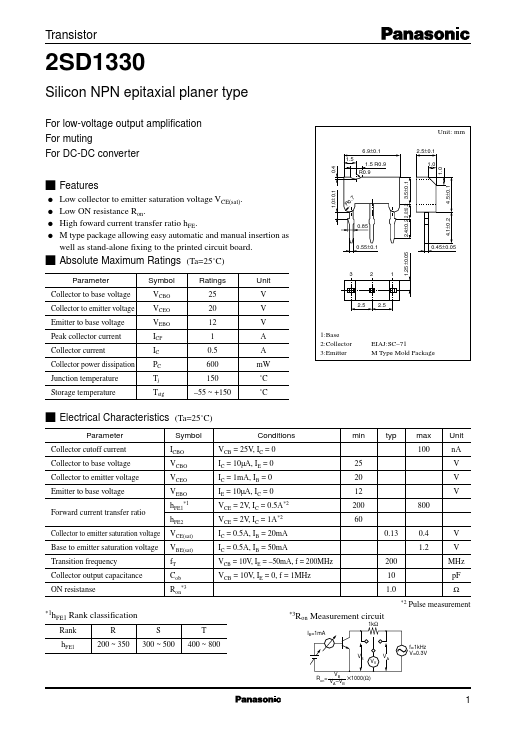
Transistor 2SD1330
Silicon NPN epitaxial planer type
For low-voltage output amplification For muting For DC-DC converter
0.4 Unit: mm
6.9±0.1 1.5 1.5 R0.9 R0.9
2.4±0.2 2.0±0.2 3.5±0.1 2.5±0.1 1.0
1.0 q q q R 0. q s Absolute Maximum Ratings
Parameter Collector to base voltage Collector to emitter voltage Emitter to base voltage Peak collector current Collector current Collector power dissipation Junction temperature Storage temperature Symbol VCBO VCEO VEBO ICP IC PC Tj Tstg (Ta=25˚C)
Ratings 25 20 12 1 0.5 600 150 –55 ~ +150 Unit V V V A A mW ˚C ˚C
1:Base 2:Collector 3:Emitter
2.5 2.5 3 2 1 EIAJ:SC–71 M Type Mold Package s Electrical Characteristics
Parameter Collector cutoff current Collector to base voltage Collector to emitter voltage Emitter to base voltage Forward current transfer ratio Collector to emitter saturation voltage Base to emitter saturation voltage Transition frequency Collector output capacitance ON resistanse
*1h (Ta=25˚C)
Symbol ICBO VCBO VCEO VEBO hFE1 hFE2 VCE(sat) VBE(sat) fT Cob Ron*3
*3R on
*1 Conditions VCB = 25V, IC = 0 IC = 10µA, IE = 0 IC = 1mA, IB = 0 IE = 10µA, IC = 0 VCE = 2V, IC = 0.5A*2 VCE = 2V, IC = 1A*2 IC = 0.5A, IB = 20mA IC = 0.5A, IB = 50mA VCB = 10V, IE = –50mA, f = 200MHz VCB = 10V, IE = 0, f = 1MHz min typ 1.25±0.05 Low collector to emitter saturation voltage VCE(sat). Low ON resistance Ron. High foward current transfer ratio hFE. M type package allowing easy automatic and manual insertion as well as stand-alone fixing to the printed circuit board. 1.0±0.1 0.85 0.55±0.1 0.45±0.05 max 100 4.1±0.2 4.5±0.