2SK614
Key Features
- 0±0.2
- 7±0.1
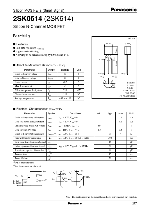
- 7±0.2 12.9±0.5 G Low ON-resistance RDS(on) G High-speed switching G Allowing to be driven directly by CMOS and TTL I Absolute Maximum Ratings (Ta = 25°C) Parameter Drain to Source voltage Gate to Source voltage Drain current Max drain current Allowable power dissipation Channel temperature Storage temperature Symbol VDS VGSO ID IDP PD Tch Tstg Ratings 80 20 ±0.5 ±1 750 150 -55 to +150 Unit V V A A mW °C °C
- 45+0.15 -0.1 2.5+0.6 -0.2 1 2 3
- 1±0.2
- 45+0.15 -0.1 2.5+0.6 -0.2 1: Source 2: Drain 3: Gate JEDEC: TO-92 EIAJ: SC-43 TO-92-A1 Package I Electrical Characteristics (Ta = 25°C) Parameter Drain to Source cut-off current Gate to Source leakage current Drain to Source breakdown voltage Gate threshold voltage Drain to Source ON-resistance Forward transfer admittance Symbol IDSS IGSS VDSS Vth RDS(on)*1 | Yfs | Coss ton
- 2 Conditions VDS = 60V, VGS = 0 VGS = 20V, VDS = 0 IDS = 100µA, VGS = 0 ID = 1mA, VDS = VGS ID = 0.5A, VGS = 10V ID = 0.2A, VDS = 15V, f = 1kHz VDS = 10V, VGS = 0, f = 1MHz min typ
- 3±0.2 max 10 0.1 Unit µA µA V V Ω mS pF pF pF ns ns 80 1.5 2 300 45 30 8 15 20 3.5 4 Input capacitance (Common Source) Ciss Output capacitance (Common Source) Reverse transfer capacitance (Common Source) Crss Turn-on time Turn-off time
- 1 *2 toff*2 Pulse measurement t on, toff measurement circuit Vout Vin = 10V 68Ω 50Ω VDD = 30V Vout Vin 10% Vin 10% 90% t = 1µS f = 1MHZ 90% V out ton toff Note) The part number in the parenthesis shows conventional part number. 277 Silicon MOS FETs (Small Signal) PD Ta 1200 1.2 Ta=25˚C 1.0 VGS=5.5V 1.0 2SK0614 ID VDS
- 2 VDS=10V Ta=25˚C ID VGS Allowable power dissipation PD (mW) 1000 800