AN7168
Overview
- Highly stable operation
- Low distortion
- Low quiescent current
- Low noise
- Low shock noise from power ON/OFF operation
- Built-in muting circuit
- Fewer external components
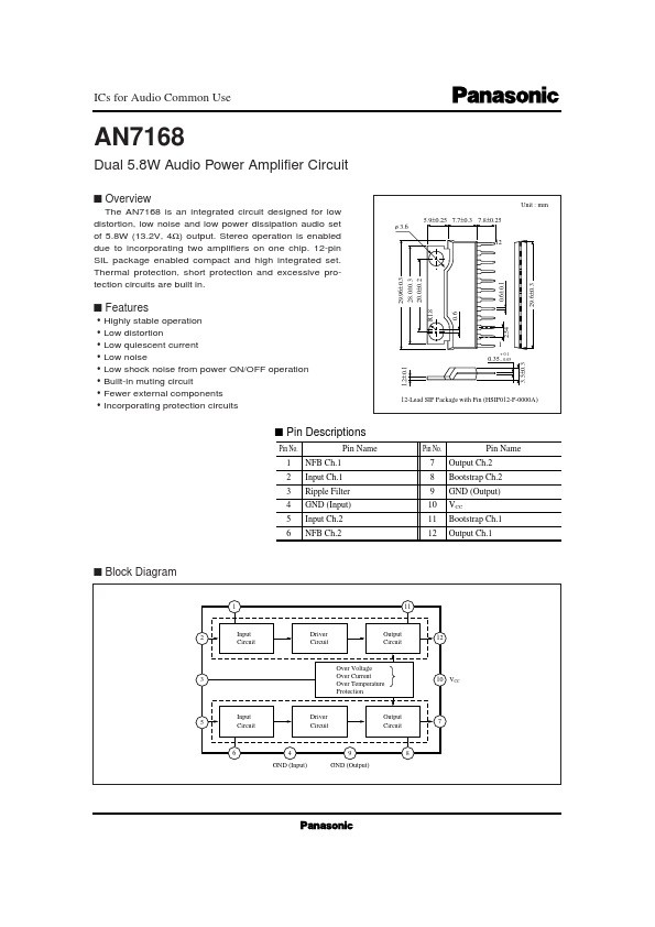
- Incorporating protection circuits s Pin Descriptions Pin No. 1 2 3 4 5 6 NFB Ch.1 Input Ch.1 Ripple Filter GND (Input) Input Ch.2 NFB Ch.2 Pin Name R1.8
- 6 1 0.35 - 0.05 1.2±0.1 3.5±0.3 + 0.1 12-Lead SIP Package with Fin (HSIP012-P-0000A) Pin No. 7 8 9 10 11 12 Pin Name Output Ch.2 Bootstrap Ch.2 GND (Output) VCC Bootstrap Ch.1 Output Ch.1 s Block Diagram 1 11 2 Input Circuit Driver Circuit Output Circuit 12 3 Over Voltage Over Current Over Temperature Protection 10 VCC 5 Input Circuit Driver Circuit Output Circuit 7 6 4 GND (Input) 9 GND (Output) 8
- 6±0.3 AN7168 s Absolute Maximum Ratings (Ta= 25˚C) Parameter Supply Voltage Supply Current Power Dissipation Note 1) Peak Supply Voltage Note 2) Operating Ambient Temperature Storage Temperature Note 1) R θ j - c = 3˚C/W Note 2) Voltage applied time = 0.2s Symbol VCC ICC PD VCC (surge) Topr Tstg ICs for Audio Common Use Rating 24 4 41.7 50 - 30 ~ + 75 - 55 ~ + 150 Unit V A W V ˚C ˚C s Electrical Characteristics (VCC = 13.2V, f = 1kHz, RL= 4Ω, Ta= 25˚C) Parameter Quiescent Circuit Current Voltage Gain Total Harmonic Distortion Symbol ICQ GV THD Vi= 0mV PO= 0.5W PO= 0.5W, f= 1kHz PO= 0.5W, f= 100Hz PO= 0.5W, f= 10kHz THD = 10% Maxim