AN7169
Overview
- Highly stable operation
- Low distortion
- Low quiescent current
- Low noise
- Low shock noise from power ON/OFF operation
- Built-in muting circuit
- Fewer external components
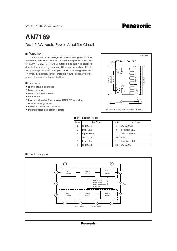
- Incorporating protection circuits s Pin Descriptions Pin No. 1 2 3 4 5 6 NFB Ch.1 Input Ch.1 Ripple Filter GND (Input) Input Ch.2 NFB Ch.2 Pin Name R1.8
- 6 1 + 0.1 0.35 - 0.05 2.54 12-Lead SIP Package with Fin (HSIP012-P-0000A)
- 2±0.1 Pin No. 7 8 9 10 11 12 Pin Name Output Ch.2 Bootstrap Ch.2 GND (Output) VCC Bootstrap Ch.1 Output Ch.1 s Block Diagram 1 11 2 Input Circuit Driver Circuit Output Circuit 12 3 Over Voltage Over Current Over Temperature Protection 10 VCC 5 Input Circuit Driver Circuit Output Circuit 7 6 4 GND (Input) 9 GND (Output) 8