B945
Key Features
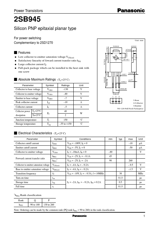
- 5±0.2
- 7±0.3 φ3.1±0.1
- 4±0.1
- 3±0.2 Solder Dip s Absolute Maximum Ratings Parameter Collector to base voltage Collector to emitter voltage Emitter to base voltage Peak collector current Collector current Collector power TC=25°C dissipation Ta=25°C Junction temperature Storage temperature Symbol VCBO VCEO VEBO ICP IC PC Tj Tstg
- 0±0.5
- 8±0.1
- 5 +0.2 -0.1
- 54±0.25 5.08±0.5 1 2 3 1:Base 2:Collector 3:Emitter TO-220 Full Pack Package(a) s Electrical Characteristics Parameter Collector cutoff current Emitter cutoff current Collector to emitter voltage Forward current transfer ratio Collector to emitter saturation voltage Base to emitter saturation voltage Transition frequency Turn-on time Storage time Fall time
- h (TC=25˚C) Symbol ICBO IEBO VCEO hFE1 hFE2* VCE(sat) VBE(sat) fT ton tstg tf IC = -2A, IB1 = - 0.2A, IB2 = 0.2A Conditions VCB = -100V, IE = 0 VEB = -5V, IC = 0 IC = -10mA, IB = 0 VCE = -2V, IC = - 0.1A VCE = -2V, IC = -2A IC = -4A, IB = - 0.2A IC = -4A, IB = - 0.2A VCE = -10V, IC = - 0.5A, f = 10MHz 30 0.13 0.5 0.13 -80 45 90 260 - 0.5 -1.5 V V MHz µs µs µs min typ max -10 -50 Unit µA µA V FE2 Rank classification Q 90 to 180 P 130 to 260 Rank hFE2 Note: Ordering can be made by the common rank (PQ rank hFE2 = 90 to 260) in the rank classification. 1 Power Transistors PC - Ta