Datasheet4U Logo Datasheet4U.com

MN195001 - Single-Chip Fax Engine LSI

Description

Functional Group For Communications Equipment Symbol A0 to 23 MD0 to 7 RD WR R/W CX SCX2 SYNCA HDRES MOD0 to 3 HALT BA IREF0 IREF1 TXLPIN TXOUT RXL IREF2 RXLPIN HPOUT AGCIN AGCOUT SHIN VREFH VREFL PLSD SO to 15 UC0 to 3 IRO1 to 4 U1ST U1RD U1RCK U1SD U1TCK U2ST U2RD U2RCK U2SD U2TCK SH1 to 4 MTA1

Features

  • Digital signal processor (DSP) block.
  • Micro ROM: 4096 × 32 bits.
  • Data RAM: 512 × 16 bits × 2 sets.
  • Machine cycle: 90 ns.
  • Parallel multiplier: 16 bits × 16 bits × → 32 bits.
  • Arithmetic and logic unit (ALU): 32-bit Facsimile peripheral circuit block.
  • Scanner/plotter interface.
  • Two USART channels.
  • Two motor control channels.
  • One thermal head control channel.
  • Programmable chip select Analog circuit block.

📥 Download Datasheet

Datasheet Details

Part number MN195001
Manufacturer Panasonic
File Size 83.57 KB
Description Single-Chip Fax Engine LSI
Datasheet download datasheet MN195001 Datasheet

Full PDF Text Transcription

Click to expand full text
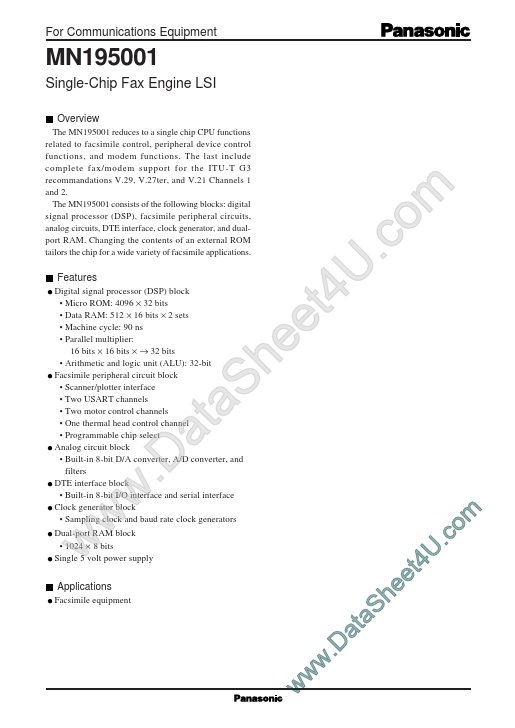
For Communications Equipment MN195001 Single-Chip Fax Engine LSI Overview The MN195001 reduces to a single chip CPU functions related to facsimile control, peripheral device control functions, and modem functions. The last include complete fax/modem support for the ITU-T G3 recommandations V.29, V.27ter, and V.21 Channels 1 and 2. The MN195001 consists of the following blocks: digital signal processor (DSP), facsimile peripheral circuits, analog circuits, DTE interface, clock generator, and dualport RAM. Changing the contents of an external ROM tailors the chip for a wide variety of facsimile applications.
Published: |