MN38663S Overview
Key Features
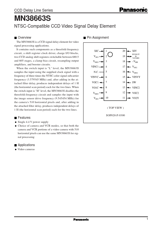
- VBB VSS2 VDD2 VINVY SW VINC2 VGC2 VO2Y
| Part | MN38663S |
|---|---|
| Description | NTSC-Compatible CCD Video Signal Delay Element |
| Manufacturer | Panasonic |
| Size | 71.00 KB |
| Part Number | Manufacturer | Description |
|---|---|---|
| CCD5061 | Fairchild Semiconductor | 6K x 128 Element / TDI-Time / Delay and Integration Sensor |
| M5227P | Mitsubishi Electric | Hi-Fi 5 Element Graphic Equalizer IC |
| M5229P | Mitsubishi Electric | Hi-Hi 7-Element Graphic Equalizer |