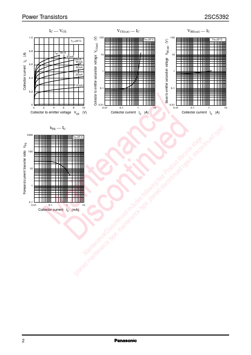
Panasonic 2SC5392
Silicon NPN Transistor
| Part No. | 2SC5392 |
|---|---|
| Datasheet | 2SC5392 Download |
| Manufacturer |  Panasonic |
| Description | Silicon NPN Transistor |
| Buy | Stock & Price |
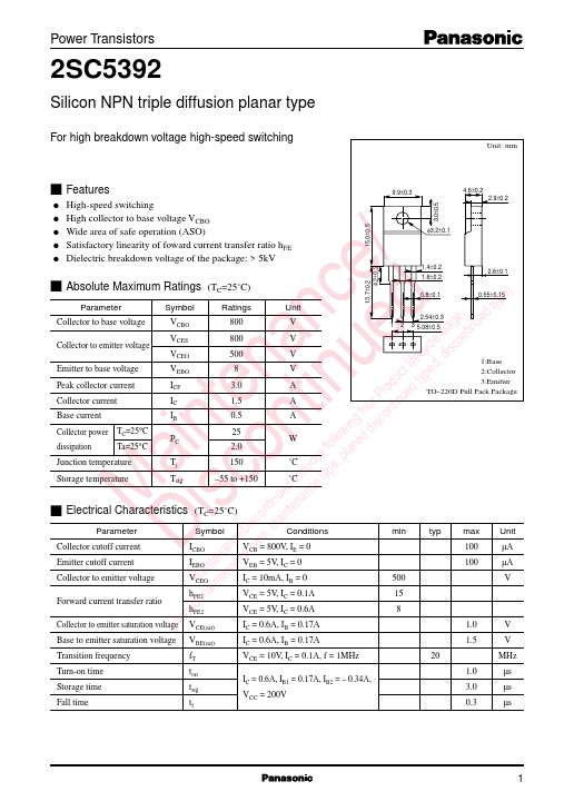
FEATURES
9.9±0.3 4.6±0.2 2.9±0.2 3.0±0.5 q High-speed switching q High collector to base voltage VCBO q Wide area of safe operation (ASO) φ3.2±0.1 q Satisfactory linearity of foward current transfer ratio hFE q Dielectric breakdown voltage of the package: > 5kV 15.0±0.5 / 1.4±0.2 2.6±0.1 1.6±0.2 e sABSOLUTE MAXIMUM RATINGS
(TC=25˚C) c type) Parameter Symbol Ratings Unit 13.7±0.2 4.2±0.2 n d tage. ued Collector to base voltage VCBO 800 V a e cle s contin Collector to emitter voltage VCES 800 V cy is VCEO 500 V n u t life ed, d Emitter to base voltage VEBO 8 V duc typ Peak collector current ICP 3.0 A te tin ur Pro tinued Collector current IC fo on Base current IB wing disc Collector power TC=25°C in n follo ned dissipation Ta=25°C PC 1.5 A 0.5 A 25 W 2.0 des , pla Junction temperature Tj 150 ˚C a o inclu type Storage temperature Tstg –55 to +150 ˚C M isc s ntinuedtenanceELECTRICAL CHARACTERISTICS
(TC=25˚C) /Disco main Parameter Symbol Conditions D ance type, Collector cutoff current te...